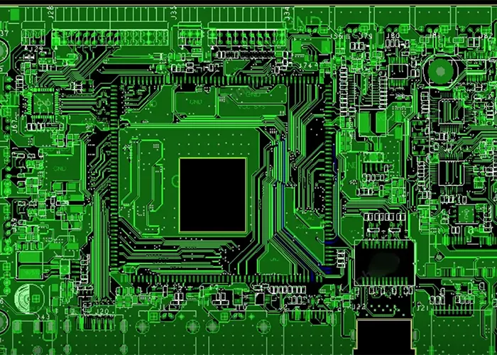
Printed Circuit Board (PCB) design is a critical stage in electronic product development, directly affecting product performance, reliability, manufacturability, and cost.
A complete PCB design workflow includes netlist import, rule configuration, component placement, routing, design verification, engineering review, and manufacturing output.
Each stage requires careful planning and strict adherence to design standards to ensure signal integrity, power distribution quality, and production success.
This guide outlines the key procedures, best practices, and precautions involved in PCB design using PowerPCB, providing a practical reference for designers seeking to develop high-quality and manufacturable PCB layouts.
Netlist Import
There are two methods for importing netlists. One is to use PowerLogic’s OLE PowerPCB Connection feature: select “Send Netlist” to apply the OLE functionality.
This ensures that the schematic and PCB remain synchronized at all times, minimizing the possibility of errors.
The other method is to load the netlist directly into PowerPCB by selecting “File” > “Import” and importing the netlist generated from the schematic.
Rule Settings
If the PCB design rules were already set during the schematic design phase, there is no need to reconfigure these rules, as the design rules are imported into PowerPCB along with the netlist.
If design rules are modified, the schematic must be updated to ensure consistency between the schematic and the PCB.
In addition to design rules and layer definitions, there are other rules that need to be configured, such as Pad Stacks, and the standard via size may need to be adjusted.
If a designer creates a new pad or via, Layer 25 must be added.
Note:
PCB design rules, layer definitions, via settings, and CAM output settings have been configured in a default startup file named Default.stp.
After importing the netlist, assign the power and ground networks to the power and ground layers according to the actual design requirements, and configure other advanced rules.
Once all rules are set, use the “Rules From PCB” function in OLEPowerPCB Connection within PowerLogic to update the rule settings in the schematic, ensuring consistency between the schematic and PCB rules.
Component Placement
After the netlist is imported, all components will be placed at the origin of the workspace, overlapping one another.
The next step is to separate these components and arrange them neatly according to certain rules—this is known as component placement.
PowerPCB provides two methods: manual placement and automatic placement.
Manual Placement
- Use the PCB Structure Dimensions tool to draw the board outline.
- Disperse the components; they will be arranged around the board outline.
- Move and rotate the components one by one, placing them within the board outline and arranging them neatly according to specific rules.
Automatic Placement
PowerPCB offers automatic placement and automatic local cluster placement; however, for most designs, the results are not ideal,
so these methods are not recommended.
Precautions
a. The primary principle of placement is to ensure routing connectivity. When moving components, pay attention to the connections of flying wires and group components that are connected.
b. Separate digital and analog components and keep them as far apart as possible.
c. Place decoupling capacitors as close as possible to the component’s VCC.
d. Consider future soldering when placing components; do not place them too densely.
e. Make extensive use of the software’s Array and Union functions to improve placement efficiency.
Routing
There are two routing methods: manual routing and automatic routing.
PowerPCB offers powerful manual routing capabilities, including automatic push-and-pull and online design rule checking (DRC).
Automatic routing is performed by the Specctra routing engine.
Typically, these two methods are used in combination, with the common workflow being manual—automatic—manual.
Manual Routing
1. Before automatic routing, manually route some critical nets first, such as high-frequency clocks and main power supplies.
These nets often have specific requirements regarding trace length, trace width, trace spacing, and shielding.
Additionally, for certain special packages, such as BGAs, automatic routing often fails to produce a regular layout, so manual routing is also necessary.
2. After automatic routing, manual routing is still required to adjust the PCB traces.
Automatic Routing
Once manual routing is complete, the remaining networks are routed by the automatic router. Select Tools->SPECCTRA to launch the Specctra router interface.
After configuring the DO file, click Continue to start the automatic routing process. Upon completion, if the routing success rate is 100%, manual adjustments can be made;
If the success rate is less than 100%, this indicates a problem with the layout or manual routing, and adjustments must be made to the layout or manual routing until all connections are successfully routed.
Precautions
a. Use the thickest possible traces for power and ground lines
b. Connect decoupling capacitors directly to VCC whenever possible
c. When setting up the Specctra DO file, start by adding the “Protect all wires” command to prevent the automatic router from rerouting manually routed traces
d. If there are mixed power planes, define the layer as a “Split/mixed Plane,” split it before routing, and use the “Plane Connect” feature in the Pour Manager to apply copper after routing is complete
e. Set all component pins to thermal pad mode by setting the “Filter” to “Pins,” selecting all pins, modifying their properties, and checking the “Thermal” option
f. When routing manually, enable DRC options and use Dynamic Route
Verification
Verification items include Clearance, Connectivity, High Speed Rules, and Power Planes. These can be checked via Tools -> Verify Design.
If high-speed rules are enabled, this check is mandatory; otherwise, it can be skipped. If errors are detected, the layout and routing must be corrected.
Note:
Some errors can be ignored, such as when part of a connector’s outline extends beyond the board boundary, which will trigger a clearance error.
Additionally, the copper layer must be re-laid each time traces or vias are modified.
Review
The review is conducted according to the “PCB Checklist,” covering design rules, layer definitions, trace widths, spacing, pads, and via settings;
Special attention should also be given to the rationality of component placement, the routing of power and ground networks, the routing and shielding of high-speed clock networks, and the placement and connection of decoupling capacitors.
If the review fails, the designer must modify the layout and routing.
Once the design passes the review, both the reviewer and the designer must sign off on it.
Design Output
PCB designs can be output to a printer or as a plot file. A printer can print the PCB in layers, facilitating inspection by both the designer and the reviewer;
The plot file is provided to the PCB manufacturer for production.
The output of the plot file is critical to the success of the design, The following section will focus on the precautions for outputting plot files.
a. Manufacturing Output Layers
Output configuration covers routing layers, including top, bottom, and intermediate layers. It also covers power layers such as VCC and GND.
Silkscreen layers include both top and bottom markings. Solder mask layers include top and bottom coverage.
Additionally, a drill file (NC Drill) must be generated.
b. Plane Connect and Layer 25 Settings
If the power layer is set to Split/Mixed, select “Routing” under the ‘Document’ section in the “Add Document” window.
Before each output of the plot file, use the “Plane Connect” function in the Pour Manager to apply copper to the PCB layout.
If set to CAM Plane, select “Plane.” When configuring the “Layer” settings, add Layer 25 and select ‘Pads’ and “Viasc” on Layer 25.
c. Aperture Value Setup
In the Device Setup window (accessed by clicking Device Setup), change the Aperture value to 199
d. Board Outline Layer Setup
When configuring the Layer settings for each layer, check the “Board Outline” option.
e. Silkscreen Layer Configuration
When configuring the Layer settings for the silkscreen layer, do not select “Part Type”; instead, select “Outline,” “Text,” and “Line” for the top (or bottom) layer and the silkscreen layer.
f. Solder Mask Via Settings
When configuring the Layer settings for the solder mask layer, selecting “Via” indicates no solder mask on the via; deselecting “Via” indicates solder mask on the via. Determine this based on the specific situation.
g. Drill File Generation Settings
When generating drill files, use PowerPCB’s default settings without making any changes
h. Final PCB Inspection and Via Design
After all plot files have been output, open them in CAM350 and print them.
The designer and reviewer inspect the outputs using the PCB Checklist. Vias serve as a key component in multilayer PCB structures.
Drilling operations account for approximately 30 to 40 percent of total PCB manufacturing cost.
Conclusion
Successful PCB design requires much more than simply connecting components.
Power and ground routing require careful attention. High-speed signal integrity, decoupling capacitor placement, and via implementation also demand close evaluation.
These factors strongly influence overall circuit performance and reliability.
Engineers follow a structured design workflow and apply industry best practices at each stage, starting from netlist import through to final manufacturing output.
This approach reduces design errors, improves production yield, and supports the successful delivery of high-performance electronic products.