Rigid-flex printed circuit boards (RFPCBs) combine the rigidity of rigid printed circuit boards (RPCBs) with the flexibility of flexible printed circuit boards (FPCB).
No longer confined to a two-dimensional plane, RFPCBs feature three-dimensional internal wiring and the ability to bend and fold freely, offering products greater integration, higher stability, lighter weight, and a smaller footprint.
Consequently, RFPCBs are increasingly replacing traditional wiring harness solutions in a growing number of projects.
This paper discusses the design, development, key manufacturing technologies, and applications of RFPCBs as replacements for wiring harness products that require limited installation space and high current capacity.
RFPCBs must satisfy both installation space constraints and high-current requirements.
Engineers simulate and design the structure and electrical performance under these conditions.
They also incorporate inner layer copper thicknesses of 70 μm or greater into the flexible board layers.
During the lamination process, risk assessments indicated that using conventional RFPCB materials and lamination processes could result in lamination voids due to the inner layer copper thickness of 70 μm or more.
Consequently, this paper addresses the lamination technology for such thick-copper RFPCBs.
Background
An assembly unit aims to improve the assembly efficiency, quality consistency, and reliability of a specific wiring harness model.
After studying industry-leading RFPCB technology for wiring harness replacement, the unit partners with the company and launches a project to develop an RFPCB product that replaces the original wiring harness model.
The project evaluated the structural design, installation space, and electrical performance requirements of the original wiring harness solution.
Engineers found that the installation space for the wiring harness was extremely limited.
Designers start the routing from the main input port.
They connect several relays along the path, and each relay requires high current ratings of 60 A, 40 A, and 20 A, respectively, under overcurrent conditions while maintaining a temperature rise of less than 40 K.
This placed higher demands on the copper thickness of the RFPCB’s inner layers.
Simulation Design
Structural Simulation
Engineers consider the positions of several functional modules and the flex circuit layout as the design basis.
They use Creo simulation software to carry out structural simulation design, focusing on the following aspects:
(1) Simulate the length of the FPCB section based on its installation within the assembly structure.
(2) Simulate the design of several relay modules according to the FPCB installation method, such as adding mechanical mounting holes and determining module orientation.
(3) Simulate the number of FPCB layers based on the number of traces between functional modules.
(4) Design circuits with different current requirements on the same flexible layer, selecting different copper thicknesses based on the current.
(5) To accommodate prolonged excessive current, the RFPCB requires structural design for both the RFPCB itself and the entire unit to ensure adequate heat dissipation.
The final structure obtained after simulation is shown in Figure 1.

Electrical Simulation
1. Simulation of RFPCB Overcurrent Technical Specifications
Product operation maintains an actual temperature rise below 40 K.
Engineers follow QJ 3103A—2011 “Design Requirements for Printed Circuit Boards,” specifically the 45 K temperature rise curve in Figure 14 on page 19.
This curve shows the relationship between trace width, cross-sectional area, operating current, and temperature rise.
Based on this standard, engineers determine the corresponding copper thickness and trace widths for the relevant load currents.
See Table 1 for specific data.
| Load Current / A | Copper Thickness (Finished) / μm | Trace Width / mm | Spacing / mm |
|---|---|---|---|
| 20 | 70 | 3.920 | 1.50 |
| 20 | 105 | 2.720 | 1.50 |
| 30 | 70 | 6.875 | 1.75 |
| 30 | 105 | 4.730 | 1.75 |
Table 1. Reference Values for Trace Width and Copper Thickness by Load Current
The relationship between load current and trace width is as follows:

In the equation: K is the correction factor, typically set to 0.055; A is the cross-sectional area of the copper cladding, in mils; T is the allowable temperature rise, in K; I is the maximum load current, in A.
Engineers select a copper thickness of 105 μm and set the allowable temperature rise to 45 K.
They then derive the functional relationship between the cross-sectional area and the load current as follows:

The equation relating the cross-sectional area A of a copper-clad strip to the line width d:

The following functional relationship between the load current I and the trace width d can be derived:

Calculations show that when the load current I = 60 A and the allowable temperature rise T = 45 K, the trace width d = 9.44 mm; when the load current I = 40 A and the allowable temperature rise T = 45 K, the trace width d = 5.40 mm.
Engineers add a margin of approximately 10% to the calculated trace width to better accommodate potential overcurrent conditions.
Table 2 shows the final design values for trace width and thickness.
| Load Current / A | Copper Thickness / μm | Trace Width / mm | Spacing / mm |
|---|---|---|---|
| 12 | 70 | 2.54 | 1.27 |
| 20 | 70 | 4.50 | 1.50 |
| 40 | 105 | 6.00 | 1.75 |
| 60 | 105 | 10.50 | 2.00 |
Table 2. Design Values for Trace Width and Copper Thickness by Load Current
2. Routing Simulation
Engineers create the PCB design using Altium Designer 10 software, as the product consists of several functional modules.
First, engineers generate the interconnections between the pins of the existing wiring harnesses and modules and draw a schematic diagram based on these connections.
Next, engineers simulate the mounting positions of the functional modules and the required FPCB circuit sections.
Engineers implement the routing combinations and connection relationships for the flexible circuit sections using vias.
Finally, engineers simulate routing in the software according to the trace width parameters obtained in the previous section and the RFPCB routing rules.
The RFPCB routing rules primarily require consideration of the following points.
(1) Traces at the rigid-flex junction should avoid sharp bends.
(2) Engineers distribute traces evenly throughout the bending area. They stagger traces on different layers and prevent vertical overlap. They also orient trace directions perpendicular to the bending area.
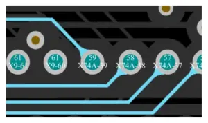
(3) Engineers design trace width changes to be gradual. They also add teardrop extensions for particularly fine traces, as shown in Figure 2.
(4) Engineers design the RFPCB layout to ensure adequate heat dissipation.
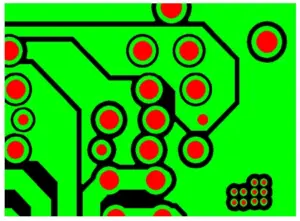
The design includes copper plating on all copper-free areas within the inner layers. Engineers also design isolated pads with isolation rings.
Figure 3 shows the pattern of one inner layer after routing is complete.
Manufacturing Process
Product Structure
Based on electrical and structural simulation designs, this RFPCB requires the use of inner layers to establish the electrical connections between the relays.
Each relay requires high overcurrent capacity, and the overcurrent calculations described above determine the design requirements.
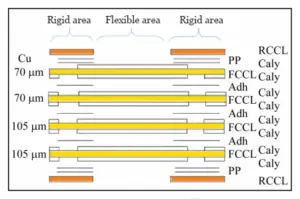
Engineers interconnect the rigid regions using several flexible traces with a copper thickness of ≥70 μm.
Figure 4 shows the product structure.
Process Flow
The manufacturing process for this product is as follows: Cutting → Inner Layer Imaging → Etching → Depth Control on the Inner Side of the Rigid Board → Inner Layer Browning → Application and Lamination of the Cover Film → Continuity Testing → Depth Control on the Outer Side of the Rigid Board → Contour Cutting → Transition Zone Treatment → Cleaning → Final Inspection.
Key Technical Challenges
Manufacturers use low-flow prepreg (PP) in conventional RFPCB production to prevent flowing prepreg from contaminating the flex zones during the lamination process.
As indicated by the product structure described above, this RFPCB features a high number of layers and thick inner-layer copper (≥70 μm).
During lamination, the adhesive in low-flow prepreg struggles to flow into the gaps of the isolation rings and the spaces between traces to fill them, resulting in lamination voids at the isolation ring locations or between traces.
Furthermore, the design requires drilling at the connection pads, so engineers position the drill holes at these delamination sites.
This creates a channel between the two network connection holes.
During the post-drilling copper plating process, the plating solution exchanges between the two holes and the channel between them, causing copper to deposit on the hole walls and within the channel.
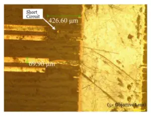
This forms a metallized connection, ultimately resulting in an electrical short circuit between the two holes’ different networks and rendering the board unusable, as shown in Figure 5.
Technical Solutions
1. PP Change
Replace the low-flow PP currently used in this RFPCB with a PP that has higher flowability, and validate its filling performance and flow distance.
2. Optimized Circuit Pattern Design Requirements
Engineers designed a test board to study the filling capability of high-flow PP.
The stack-up design of the test board matches that of the RFPCB, and the requirements for the inner layer circuit patterns and drill hole design are as follows: hole spacing of 0.1–1.0 mm, with isolation ring sizes of 0.10, 0.15, 0.20, 0.30, 0.35, and 0.50 mm.
Engineers also designed pads on the RFPCB surface layer. During lamination, the process used high-flow PP, and engineers tested electrical continuity between the pads.
Test results indicated that short circuits occurred when hole spacing was ≤0.3 mm and the single-side isolation ring width was 0.1 mm, while all other locations passed the continuity test.
Based on these findings, engineers redesigned the isolation rings and hole spacing for this RFPCB type to meet the requirements of a 0.25 mm single-side isolation ring and a hole spacing of ≥0.4 mm.
3. Optimization of the PP Window Design
To ensure that PP adhesive does not seep into the flex zone, the flow value of the PP adhesive was verified using the resin flow test method specified in IPC TM-650 T2.3.17.2 for “non-flowing” adhesive patches.
Engineers recorded the test results in Table 3. Based on the flow value test results, they designed the size of the window in the PP flex zone accordingly.
| No. | Hole Diameter After Pressing / mm | Flow Value / mm |
|---|---|---|
| 1 | 5.243 | 0.757 |
| 2 | 5.185 | 0.815 |
| 3 | 5.322 | 0.678 |
| 4 | 5.320 | 0.680 |
| 5 | 5.434 | 0.566 |
| 6 | 5.319 | 0.681 |
| 7 | 5.235 | 0.765 |
| 8 | 5.189 | 0.811 |
Table 3. PP Flow Value Test Results
Product Manufacturing Process
Engineers implemented the design outlined in Table 3 and carried out a small-batch production run of the PCB manufacturing process to verify its effectiveness.
1. Laminating Process
Following lamination, engineers inspected the PCB surface.
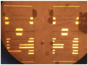
A higher-flow PP adhesive filled the gaps between traces more thoroughly, producing a smoother surface, as shown in the comparison in Figure 6.
An industry-standard method added a carrier film in the flexible areas to prevent the highly fluid PP adhesive from contaminating those regions.

2. Drilling Process
After drilling, engineers performed cross-sectional analysis on the two holes closest to the previously observed voids and micro short-circuit resistance areas.
The resin fully filled the interlayer gaps, and no voids were detected, as shown in Figure 7.
3. Electrical Continuity Testing
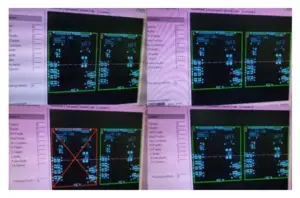
Engineers tested a total of eight small components during the PCB electrical continuity test.
Except for one component that the previous process had already scrapped, all components passed the test, as shown in Figure 8.
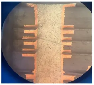
Engineers analyzed a cross-section of the plated-through hole at the narrowest point of the isolation ring and found no lamination voids between the holes. The cross-section is shown in Figure 9.
4. Removing the Rigid Plate
Result after removal: After removing the scrap rigid plate from the flexible area, there was no excess adhesive in the flexible area, and the surface flatness was good.
Following this improvement, no PP adhesive flowed into the flexible area.
Application Scenario
Engineers conducted functional testing of the RFPCB at the client’s site, and the results met design requirements, confirming that the RFPCB can fully replace wire harness products.
During the final assembly process, the RFPCB offers the following five advantages:
① Weight is approximately 60% lighter than that of wire harnesses;
② The process reduces manual labor and achieves high product consistency;
③ The process increases production efficiency by approximately 8 times;
④ The system eliminates assembly errors, resulting in a 0% error rate;
⑤ The structural components of the finished unit fit tightly together, saving a significant amount of space.
Conclusion
Overcurrent capacity simulation follows the requirements of QJ 3103A—2011 “Design Requirements for Printed Circuit Boards.”
Engineers use Creo simulation software for structural design. This approach enables the development of an RFPCB product featuring 105 μm and 70 μm thick copper layers.
During the manufacturing process, we addressed lamination voids encountered by optimizing the thick copper lamination process, successfully developing a 105 μm thick copper RFPCB product.
The product has been verified through actual testing by the client and can simultaneously meet the requirements of a small installation footprint and high overcurrent capacity.
The successful development of this thick copper product provides a new technical solution for replacing cables with RFPCBs.
It offers technical support for similar products that require high current capacity and have limited installation space.
Engineers have successfully applied this technology to similar thick-copper projects, and such thick-copper RFPCBs can meet the demands of high-current products.