With the rapid development of electronic devices, printed circuit boards (PCBs) have evolved from single- and double-sided boards to multilayer boards, utilizing blind and through-holes (hereinafter referred to as “blind-through holes”) to enable signal transmission and interconnections.
In the processing of blind-via holes, plasma equipment is typically used to clean the hole walls, followed by direct metallization or electroplating after chemical copper plating to achieve metallized conductivity.
In the metallization via processing workflow, insufficient or excessive treatment of the hole walls will directly affect the reliability of interlayer electrical connections.
This paper focuses on flexible printed circuit boards (FPCBs) containing multilayer blind-through-holes and analyzes the effect of plasma treatment parameters on the extent of adhesive etching on the hole walls.
Current Issues
During functional testing—such as open-circuit and short-circuit tests—of a batch of multilayer FPCBs featuring through-hole designs, some products exhibited abnormal network resistance values.
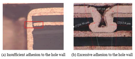
Cross-sectional analysis of the defective products revealed inner connection defects (ICDs) in the via walls, characterized by two phenomena: insufficient adhesive bonding and excessive bonding, as shown in Figure 1.
ICD issues impact the electrical performance of printed circuit boards. Minor ICDs cause signal distortion and transmission delays.
Severe ICDs trigger critical failures such as open circuits and short circuits, which render the product inoperable.
Excessive etching weakens the bond between the copper foil and the substrate at the via walls.
This weakening makes the via walls more susceptible to cracking at corners or bends.
Such damage reduces the mechanical strength and durability of the FPCB and degrades signal transmission quality.
Analysis of Causes
A single product design may include blind and through holes with different diameters.
In such cases, the total plasma etching volume directly affects ICD formation on the hole walls as well as excessive etching of the adhesive layer.
If the total etching volume is too small, residual adhesive on the hole walls cannot be effectively removed;
If the total etching volume is too large, the adhesive layer on the hole walls is over-etched.
The etching rate of plasma within the hole is related to temperature, power, and vacuum level.
The study designed experimental protocols based on conventional process parameters, including the flow rate of the key plasma gas carbon tetrafluoride (CF₄) and exposure time.
It used these parameters to verify resin etching behavior on the walls of blind through-holes with different diameters.
It also analyzed the results to identify potential process improvement strategies.
Test Plan Design
Test Product Structure
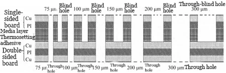
The test product selected for validation and improvement is a problematic 3-layer FPCB with a stack-up consisting of a single-sided board + dielectric layer + double-sided board.
The dielectric layer is a 20 μm thermosetting adhesive. The product design includes blind and through-holes ranging from 75 to 300 μm, as shown in Figure 2.
Test Principle and Operating Process
The principle of plasma equipment is that CF₄ and oxygen (O₂) gases are ionized into a plasma state.
Contaminants on the hole walls (primarily resin) contain a significant amount of organic matter (mainly C, H, and O elements).
During the plasma process, oxygen reacts with certain elements to form CO₂ and H₂O, which subsequently volatilize and are extracted.
At the same time, corrosive gaseous plasma containing hydrogen fluoride—a byproduct of CF₄—etches away the molecular chains of the remaining adhesive, achieving effective adhesive removal.
The plasma cleaning process consists of three main stages: heating, operation, and activation.
(1) Heating Stage: The primary function is to warm up the system and raise the temperature, preparing for the next stage to increase the etching rate.
(2) Working Stage: The primary function is to etch the resin on the hole walls by ionizing plasma using gases such as CF4, thereby cleaning the hole walls.
(3) Activation Stage: The primary function is to neutralize CF4 and other harmful gases within the chamber to ensure operator safety.
Common plasma parameters for through-hole cleaning in printed circuit board (PCB) processing are shown in Table 1.
| Stage | O₂ (cm³·min⁻¹) | N₂ (cm³·min⁻¹) | CF₄ (cm³·min⁻¹) | Power (kW) | Time (min) | Vacuum Degree (Torr) | Temperature (°C) |
|---|---|---|---|---|---|---|---|
| 1 | 2000 | 500 | 0 | 4 | 3 | 0.25 | 70 |
| 2 | 2000 | 200 | 150 | 3.5 | 10 | 0.25 | 70 |
| 3 | 0 | 2000 | 0 | 3 | 2 | 0.25 | 40 |
Table 1. Common Through-Hole Plasma Parameters
Test Equipment and Data Collection
Test Equipment: Metallographic microscope, vertical plasma etcher, laser drilling machine.
Data Collection: Once plasma etching is completed, the operator removes three test plates from the upper, middle, and lower regions of the plasma etcher chamber, taking one plate from each region.
Each region therefore provides a single representative test plate for evaluation.
After copper plating and copper electroplating, each test plate underwent micro-sectioning using holes of different diameters, selecting one hole at each corner and one at the center.
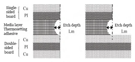
A metallographic microscope then measured the etching depth (Lm) of the adhesive layer on the hole walls, as shown in Figure 3.
The study collected a total of 15 data sets for each hole diameter.
Analysis of Test Results
Etching Effect on Through-Holes
Among the nine schemes, Schemes 3, 5, and 7 met the etching volume requirements and exhibited no ICD issues.
The process established the optimal parameter range by setting the total CF₄ dosage to 1,500–2,000 cm³.
It also defined the exposure time range as 5–15 minutes, while adjusting the actual exposure time in accordance with the total CF₄ dosage.
| Plan | CF₄ Flow Rate (cm³·min⁻¹) | Treatment Time (min) | Total CF₄ Amount (cm³) | Hole Type | 75 μm Max | 75 μm Min | 150 μm Max | 150 μm Min | 300 μm Max | 300 μm Min | ICD on Hole Wall | Etch Depth (μm) |
|---|---|---|---|---|---|---|---|---|---|---|---|---|
| 1 | 100 | 5 | 500 | Through Hole | 1.9 | 0.5 | 3.5 | 1.2 | 4.6 | 1.7 | ICD exists in all holes | <15 |
| Blind Via | 1.5 | 1.1 | 3.3 | 1.8 | 4.2 | 2.3 | ||||||
| 2 | 100 | 10 | 1000 | Through Hole | 4.9 | 1.6 | 6.6 | 2.9 | 7.6 | 3.4 | ICD exists in 75 μm through holes | <15 |
| Blind Via | 4.0 | 1.7 | 5.7 | 2.8 | 6.6 | 3.2 | ||||||
| 3 | 100 | 15 | 1500 | Through Hole | 6.8 | 2.0 | 8.5 | 2.6 | 9.5 | 3.0 | No | <15 |
| Blind Via | 6.0 | 3.0 | 7.8 | 3.5 | 8.8 | 3.9 | ||||||
| 4 | 200 | 5 | 1000 | Through Hole | 5.5 | 3.2 | 7.1 | 4.0 | 8.2 | 4.5 | ICD exists in 75 μm through holes | <15 |
| Blind Via | 5.0 | 3.6 | 6.6 | 3.9 | 7.6 | 4.4 | ||||||
| 5 | 200 | 10 | 2000 | Through Hole | 10.6 | 4.3 | 11.3 | 4.7 | 12.9 | 5.2 | No | <15 |
| Blind Via | 9.9 | 4.7 | 10.6 | 5.5 | 12.0 | 6.0 | ||||||
| 6 | 200 | 15 | 3000 | Through Hole | 13.9 | 5.3 | 14.5 | 5.8 | 15.6 | 6.3 | No | 300 μm through holes >15 |
| Blind Via | 12.8 | 5.8 | 14.2 | 6.3 | 15.3 | 6.8 | ||||||
| 7 | 300 | 5 | 1500 | Through Hole | 7.6 | 3.3 | 9.3 | 4.6 | 10.3 | 5.1 | No | <15 |
| Blind Via | 6.9 | 4.0 | 8.6 | 5.0 | 9.8 | 5.5 | ||||||
| 8 | 300 | 10 | 3000 | Through Hole | 14.9 | 5.5 | 16.3 | 6.2 | 17.7 | 6.7 | No | 150/300 μm through holes >15 |
| Blind Via | 14.0 | 5.6 | 15.1 | 6.4 | 16.1 | 6.9 | ||||||
| 9 | 300 | 15 | 4500 | Through Hole | 19.6 | 6.6 | 21.0 | 8.0 | 22.6 | 8.5 | No | All >15 |
| Blind Via | 18.5 | 7.7 | 20.6 | 8.2 | 21.3 | 8.7 |
Table 2. Cross-Validation Test Results for Different Factors
| Scheme | Total CF₄ Dose (L/cm³) | Hole Type | Etch Depth (μm) | ICD on Hole Wall | Result Evaluation |
|---|---|---|---|---|---|
| 1 | 500 | Through hole / Blind hole | < 15 | ICD present in all holes | Does not meet requirements |
| 2 | 1,000 | Through hole / Blind hole | < 15 | ICD present in 75% of blind holes | Blind holes do not meet requirements |
| 3 | 1,500 | Through hole / Blind hole | < 15 | No | Meets requirements; better uniformity |
| 4 | 1,000 | Through hole / Blind hole | < 15 | ICD present in 75% of blind holes | Blind holes do not meet requirements |
| 5 | 2,000 | Through hole / Blind hole | < 15 | No | Meets requirements; slightly poorer uniformity |
| 6 | 3,000 | Through hole / Blind hole | Hole diameter 300 μm; through holes >15 μm | No | Does not meet requirements |
| 7 | 1,500 | Through hole / Blind hole | < 15 | No | Meets requirements; good uniformity |
| 8 | 3,000 | Through hole / Blind hole | Hole diameters 150/300 μm; through holes >15 μm | No | Does not meet requirements |
| 9 | 4,500 | Through hole / Blind hole | All >15 μm | No | Does not meet requirements |
Table 3. Evaluation of Different Plasma Treatment Conditions
Plasma Etching Results for Through-Holes
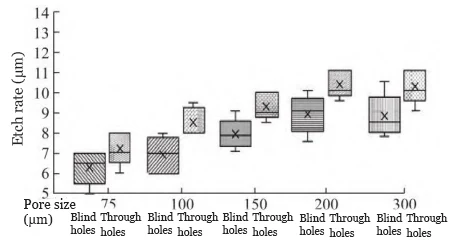
Tests used the optimal plasma parameters for through-holes (Scheme 3) validated in Section 4.1.
The process followed the data collection procedure, completing plasma etching, copper plating, and electroplating before measuring the amount of resin etched on the hole walls.
The results appear in Figure 4.
Summary
(1) For both blind holes and through holes, as the hole diameter increases, the flow rate of the plasma gas within the hole increases, and the amount of polymer etching inside the hole shows a gradual upward trend.
When the hole diameter is 200 μm and 300 μm, the amount of polymer etching is comparable and remains stable.
This indicates that once the hole diameter exceeds a certain size, the etching rate per unit area of the polymer reaches saturation;
Even if other flow rates within the hole increase with the hole diameter, the etching rate on the hole walls will not continue to increase.
(2) For the same aperture size, the etching rate of the resin in through-holes is slightly higher than that in blind holes, and the etching uniformity (box plot width) is superior to that of blind holes.
Through-holes allow plasma to fully penetrate the structure, enabling CF₄ and other ionized species to reach the entire hole surface and drive more active resin etching.
Blind holes function as single-sided channels, so they prevent complete plasma exchange compared with through-holes, which results in lower etching rates and reduced uniformity.
Conclusion
This study investigated the relationship between the total amount of CF₄ used in plasma etching and the etch rate of blind through-holes with different diameters.
Within a certain range of hole diameters, the study found that the etch rate increases as the hole diameter increases.
When designing plasma processing for products containing blind through-holes of different diameters, a total CF4 exposure volume of 1,500–2,000 cm³ ensures that no ICD issues occur for all hole diameters and that etching depth remains <15 μm.
The factor step spans limited the full reflection of some parameter results during testing.
Based on the experimental results, the process can extend the total CF₄ exposure to more than 1,000 cm³, but it must not exceed 3,000 cm³.
Users must verify the plasma cleaning effects corresponding to different total CF₄ exposure parameters before making a selection.