With the continuous advancement of electronic circuit technology, printed circuit boards (PCBs) are evolving toward higher-density circuits.
As component sizes in printed circuit board assemblies (PCBAs) continue to shrink and product integration increases, the impact of environmental factors on PCBAs is becoming increasingly significant.
The industry extensively uses conformal coatings on high-end circuit boards in high-tech fields such as automotive, military, and aerospace.
These coatings significantly improve the quality of PCBA products.
While conformal coatings offer numerous advantages, defects such as shrinkage, delamination (poor adhesion), and bubbles frequently occur during production, severely compromising protective performance.
Shrinkage and delamination on the solder mask surface are particularly prominent.
To address these issues, the PCBA side typically employs methods such as modifying the coating process, optimizing oven temperature profiles, cleaning the PCB, or switching to conformal coatings with lower surface tension.
This study proposes a process to improve the surface energy of the PCB solder mask, thereby mitigating delamination on the solder mask surface.
The study also verifies that this method has no adverse effects on the physicochemical properties of the solder mask.
Analysis of the Causes of Shrinkage and Delamination of Solder Mask Coating on PCBs
The solder mask layer on a PCB serves as an insulating layer to protect the surface copper foil.
It typically has a smooth, hydrophobic surface with low surface energy.
When applying conformal coating to a PCBA, if the surface tension of the conformal coating exceeds the surface energy of the solder mask, the coating will fail to effectively wet the solder mask surface, leading to shrinkage or delamination.
The wetting behavior between the solder mask surface and the conformal coating is closely related to surface tension (surface energy).
Solder mask ink primarily consists of epoxy resin and other additives; the surface energy of cured epoxy resin can reach 45 mN/m, but the addition of additives reduces it to 28–32 mN/m.
Conventional conformal coating has a surface tension of 32–36 mN/m, which is higher than the surface energy of cured solder mask, preventing the conformal coating from effectively wetting the solder mask surface, as shown in Figure 1.
When the surface energy of a solid exceeds the surface tension of a liquid, the liquid exhibits good wetting on the solid surface.

Test Design
Test Materials, Equipment, and Instruments
Main Materials: Glossy ink, semi-matte ink, emery;
Main Equipment: Solder mask development line, solder mask laser direct imaging (LDI) exposure unit, oven, plasma equipment, sandblasting line, dyne pen, 3M tape.
Experimental Design and Protocol
This experiment primarily investigates changes in the surface energy of cured glossy and semi-matte solder mask inks following different surface treatment methods, as well as changes in surface energy after storage at room temperature for varying durations.
Given the solder masks’ acid- and alkali-resistance after curing, the team employed two surface treatment techniques: sandblasting and plasma modification.
They established corresponding sandblasting parameters for three surface coating conditions: thick gold plating, thin gold plating, and electroless nickel-gold plating, considering the relationship between sandblasting pressure and surface coating method.
The team determined modification parameters based on experience with plasma modification of polytetrafluoroethylene (PTFE) products.
On this basis, this study designed a set of cross-experimental protocols (see Table 1).
| No. | Ink Type | Surface Treatment Method | Condition | No. | Ink Type | Surface Treatment Method | Condition |
|---|---|---|---|---|---|---|---|
| 1 | Gloss Ink | Sandblasting | 0.5 kg/cm² | 5 | Matte Ink | Sandblasting | 0.5 kg/cm² |
| 2 | — | Sandblasting | 1.0 kg/cm² | 6 | — | Sandblasting | 1.0 kg/cm² |
| 3 | — | Sandblasting | 1.5 kg/cm² | 7 | — | Sandblasting | 1.5 kg/cm² |
| 4 | — | Plasma Treatment | 40 min | 8 | — | Plasma Treatment | 40 min |
Table 1. Cross-Validation Experimental Plan for Surface Energy Improvement
Test Results and Analysis
Interpretation of Ink Surface Energy Test Results
To ensure better wetting and adhesion of the conformal coating on the solder mask surface, the surface energy of the solder mask must exceed the surface tension of the conformal coating (i.e., it must reach 38 mN/m);
Therefore, this test uses a 38# dyne pen for measurement.
The team measured the two solder mask inks that had not undergone surface energy enhancement using a 38# dyne pen.
Within 3 seconds, the ink marks contracted rapidly, showing that the surface energy of both untreated solder mask inks was low, below 38 mN/m.
Test Results
1. Test Board Fabrication Process
Two types of ink were processed according to the standard procedure of “pretreatment → screen printing → pre-baking → exposure → development → post-curing” to produce cured solder mask test boards.
Surface energy enhancement treatments were performed according to the schemes in Table 1:
combining Scheme 1 with Scheme 5, Scheme 2 with Scheme 6, and Scheme 3 with Scheme 7, three sets of sandblasting parameters (1.5, 1.0, and 0.5 kg/cm²) were established for thick gold plating, thin gold plating, and chemical nickel-gold plating, respectively;
Schemes 4 and 8 were processed using a 40-minute plasma modification.
2. Test Results
(1) Initial Test Results
After processing each sample according to the established procedure, measurements were taken using a 38# dyne pen. The comparative results are shown in Table 2.
The tests show that sandblasting has a limited effect on increasing the surface energy of glossy solder mask inks.
Sandblasting does not significantly improve the surface energy of matte inks. Plasma modification significantly increases surface energy.
| Scheme | Condition | Result |
|---|---|---|
| 1, 2, 3 | Gloss Ink + Sandblasting Treatment | At different pressure levels, the test plates showed uniform ink leveling within 3 seconds. No ink shrinkage was observed. Surface energy was 38 mN/m. |
| 5, 6, 7 | Matte Ink + Sandblasting Treatment | Ink leveling time varied under different sandblasting pressures. At lower pressure, ink shrinkage was more noticeable. Surface energy was below 38 mN/m. |
| 4, 8 | Gloss & Matte Ink + Plasma Treatment | Ink leveled within 3 seconds and showed an outward spreading trend. Surface energy exceeded 38 mN/m. |
Table 2. Comparison of Test Results
(2) Recording Surface Energy Test Results at Different Time Points
After completing PCB fabrication, the team typically vacuum-packs the boards. They store them for a period before assembly.
To investigate the durability of the surface energy improvement, this experiment simulated a room-temperature environment by storing the boards for 15 days.
The team selected Schemes 3, 4, and 8 for comparative testing. They measured every 1 to 3 days using a 38-dyne pen. Table 3 shows the results.
| Solution | Conditions | Results |
|---|---|---|
| 3 | Gloss oil coating + spray treatment | For different batches of samples, ink can reliably adhere to the solder mask surface within 3 hours, and the surface energy remains basically at 38 mN/m. However, from day 2 to day 15, observations show that with each test interval extending, ink shrinkage occurs. |
| 4, 8 | Gloss oil coating + plasma treatment | Ink can adhere to the solder mask surface within 3 hours, and the distribution of ink droplets is relatively uniform. From observations between day 2 and day 15, the ink droplets spread evenly in all directions, but as time is extended, the spreading distance decreases, indicating that the treatment effect weakens over time. |
Table 3: Comparison of Surface Energy Retention Over Time for Solder Mask
Schemes 3 (Sandblasting):
Physically increases the surface roughness of the solder mask to expand the contact area between the solder mask and the ink, thereby increasing the surface energy of the solder mask.
However, over time, subtle changes occur on the solder mask surface, causing the ink to shrink.
Schemes 4 and 8 (Plasma Modification) Increase surface energy by grafting -H or other hydrophilic functional groups onto the solder mask surface; however, prolonged exposure to air causes the modification to gradually fail.
These results indicate performance at room temperature. Diffusion distance decreases over time.
Plasma modification outperforms sandblasting. Its effectiveness lasts for more than 15 days under ambient conditions.
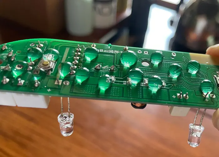
(3) Application Results of the Triple-Protection Coating
When the triple-protection coating is applied to products treated with plasma-modified glossy ink, it distributes evenly across the solder mask surface.
No defects occur, such as shrinkage or delamination. Figure 2 shows the result.

Performance Testing
Based on previous test results, the team selected test boards for Solutions 3, 4, and 8 for further performance evaluation.
Appearance
After sandblasting and plasma modification, both solder mask surfaces showed no defects.
No bubbling, cracking, or discoloration occurred. The appearance requirements specified in the GJB 9491 standard were met.
Changes in Solder Mask Thickness
Prior to testing, the solder mask thickness on the test board was 23.44 μm.
After applying Schemes 3 and 4 and testing using Schemes 3, 4, and 8, the thicknesses were 22.82, 24.05, and 23.44 μm, respectively.
The solder mask thickness remained within the range of (23.00 ± 1.00) μm before and after testing.
No significant change occurred. The thickness met the ≥18.00 μm requirement specified in GJB 9491.
Relevant Reliability Tests
The team conducted reliability tests on the test board. Test results appear in Table 4.
| No. | Evaluation Item | Test Method | Evaluation Criteria | Evaluation Result |
|---|---|---|---|---|
| 1 | Adhesion | Cross-hatch test on copper foil solder mask layer using a utility knife; 3M tape applied and peeled vertically | No flaking or ink removal | Pass |
| 2 | Heat Resistance | Immersion at (288 ± 5) °C for 10 seconds, repeated 3 times | No blistering, peeling, or cracking | Pass |
| 3 | Reflow Soldering Test | Reflow soldering 5 times (peak temperature 265 °C) | No blistering or cracking | Pass |
| 4 | Thermal Shock | Temperature cycle from -40 °C to +140 °C, holding 15 minutes at each extreme, 1000 cycles | No blistering or cracking | Pass |
Table 4: Summary of Relevant Reliability Tests
Conclusion
This paper proposes a process for modifying the surface energy of the PCB solder mask.
Comparative testing and validation demonstrate effectiveness. Forty minutes of plasma modification increase surface energy.
Both glossy and matte solder masks reach over 38 mN/m. Coating requirements for conventional conformal coatings are met.
Performance test results show an increase in surface energy. The appearance and thickness remain unchanged. Reliability requirements are fully satisfied.