As ChatGPT drives surging demand for computing power, the PCB (Printed Circuit Board)—a cornerstone of the computing power industry chain—is poised for significant growth.
Against this backdrop, AI-enabled PCBs have emerged as an innovative product resulting from the deep integration of AI technology and circuit design.
By integrating advanced algorithms with precision circuit architectures, these PCBs endow various smart devices with powerful edge computing capabilities and precise control.
Increasing Design Complexity and Manufacturing Challenges
As electronic products continue to move toward higher integration, PCB design is characterized by increasingly fine and dense circuit patterns, accompanied by a continuous increase in the number of routing layers, greater board thickness, and smaller via diameters.
The thickness-to-diameter ratio has increased from the original 20:1 to 50:1 or even higher, posing greater technical challenges for PCB manufacturing processes.
These drastic changes in geometric parameters present unprecedented technical challenges for PCB manufacturing.
They particularly affect micro-via machining precision, interlayer alignment error control, and material adaptability optimization.
Urgent technical bottlenecks in these areas await breakthroughs.
Rise and Future of Z-Axis Interconnect PCBs
Notably, the rapid iteration of artificial intelligence and AI server technologies profoundly reshapes the PCB industry landscape.
It gives rise to Z-axis interconnect printed circuit board products.
These products feature high aspect ratios, ultra-fine circuit lines, and high-density integration.
Currently, the manufacturing technology for Z-interconnected printed circuit boards still faces numerous challenges, including high process complexity and difficulties in developing new materials.
However, amid the global wave of industrial intelligent transformation, the electronic components industry is accelerating its evolution toward miniaturization, high power density, environmental sustainability, and module integration.
It is foreseeable that Z-axis interconnect PCBs will play an increasingly pivotal role in the future of smart technology.
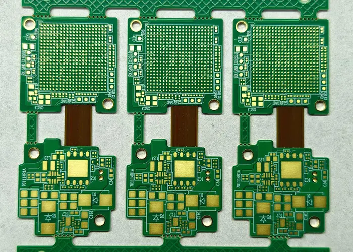
This article focuses on this technological field, systematically exploring key manufacturing techniques—including the fabrication process, production challenges, and improvement measures—for localized “convex-type” Z-axis interconnect PCBs (Figure 1), with the aim of providing valuable reference for the broader PCB industry.

Basic Characteristics and Technical Specifications of Z-Axis Interconnect PCBs
The physical diagram and basic characteristics of the localized “convex-type” Z-axis interconnect printed circuit board described in this article are as follows.
| Item | PCB Board 1 | PCB Board 2 |
|---|---|---|
| Number of layers | 28L | 16L |
| Stacking characteristics | N+N (14L + 14L) | 7-stage UHDI (7+2+7) |
| Panel grade | Grade M7 | Grade M8 |
| Plate thickness | 4.0 mm | 1.4 mm |
| Surface treatment | Nickel-plated gold | Nickel–palladium–gold |
| Finished dimensions | 400 × 400 mm | 140 × 140 mm |
| Properties After Transient Liquid-Phase Sintering and Pressing | 1. The theoretical interlayer thickness (d) between two PCBs in transient liquid-phase sintering is 101.6 μm 2. The via size (a) in transient liquid-phase sintering is 254 μm 3. The connection pad size (c) in transient liquid-phase sintering is 457.2 μm 4. The pad pitch (e) for different networks in transient liquid-phase sintering is 800 μm 5. The interlayer misalignment control for two PCBs is 101.6 μm | |
| Technical Indicators | 1. No wrinkles or bubbles between PET film, pre-cured PP laminate, and PCB; laminate must adhere perfectly without looseness 2. Hole diameters of laser-drilled holes in PET film + pre-cured PP laminate must meet quality requirements 3. Screen-printed copper paste must be void-free; no leakage or adhesion between holes 4. Z-axis alignment deviation between parent and child boards must be < 101.6 μm 5. No cracks at connection points after transient liquid-phase sintering; pore size < 25.4 μm 6. No voids after sintering; product reliability must meet IPC standards | |

Design of a Transient Liquid-Phase Sintering Process for Z-Axis Interconnects
Process Design
Z-axis interconnect printed circuit boards (PCBs) are an advanced PCB structure that utilizes transient liquid-phase sintering technology to achieve vertical interconnections.
This technology constructs a three-dimensional interconnect architecture by forming reliable vertical electrical connections via intermetallic compounds at specific pad areas on two or more independently manufactured sub-boards.
This paper focuses on the core process steps for fabricating a printed circuit board with localized “convex” Z-axis interconnections.
This involves using PCB 1, which has undergone surface treatment, as the substrate for screen-printing copper paste; subsequently, it is laminated with PCB 2—which has independently undergone surface treatment, molding, electrical testing, and visual inspection—to form the interconnection.
Due to space limitations, the processes for the two sub-boards are not elaborated upon here; the specific design is as follows:

Technical Features and Advantages
(1) One or more sub-boards are mounted on one or both sides of a parent PCB. Holes are laser-drilled into a pre-cured or semi-cured PP sheet, and TLPS solder paste (copper paste) is dispensed into these holes.
After lamination, this process establishes metal connections between the pads of different PCBs; the final product forms a locally “convex” Z-axis interconnect printed circuit board.
(2) Before transient liquid-phase sintering lamination, both PCB 1 and PCB 2 have completed solder mask application, marking, and surface treatment; additionally, PCB 2 must undergo further processes, including forming, electrical testing, and visual inspection.
Therefore, PCB 1 and PCB 2 can be manufactured through separate design processes without interfering with each other, requiring only that their target expansion rates be controlled within a specific range.
(3) For PCB 1, the areas corresponding to the transient liquid-phase sintering zones on PCB 2 do not undergo solder mask application, marking, or surface treatment.
Additionally, PCB 2 requires a browning treatment before transient liquid-phase sintering lamination.
Due to the lamination process, surface treatment processes such as electroless nickel-gold, nickel-palladium-gold, and electroplated nickel-gold—which offer high flatness and do not affect soldering after high-temperature processing—are prioritized.
(4) Given the design diversity and independence of PCB 1 and PCB 2, the primary advantages of Z-axis interconnect products lie in the fabrication of boards with ultra-high aspect ratios (AR) and the reduction of lamination cycles for high-order HDI boards; simultaneously, they enhance the spatial depth of the PCB.
Process Key Points, Difficulties, Control, and Production
Vacuum Quick Pressing
Vacuum quick pressing serves to create a certain degree of adhesion between the PP and the PCB board, as well as between the PET film and the PP, in preparation for subsequent processing.
The key process quality indicators are: no wrinkles or bubbles between the PET film, PP, and PCB. The key control measures are as follows:
(1) Vacuum level > 700 mm Hg: pre-pressing time and pressure: 10 s × 20 kg.
(2) Hot pressing temperature: 125°C–140°C (depending on the dynamic viscosity of the selected PP); hot pressing time: 60–90 s (depending on its curing temperature).
Hot pressing pressure: 100 bar (maximum pressure).
(3) Before hot pressing, use a lint roller to remove foreign particles from the surface of the PCB and the vacuum bag to ensure cleanliness.
(4) The hot pressing stack-up, from bottom to top, is as follows (Figure 3): release film—PCB—PP—PET film (ensuring coverage of the sintering area)—release film

For the product studied in this paper, transient liquid-phase sintering lamination is performed only in specific areas, and the PP must be milled to the appropriate size.
To ensure the reliability of the transient liquid-phase sintering lamination and to prevent interlayer slippage, perform two vacuum rapid-pressing cycles on PCB 1.
During the first vacuum rapid pressing, fully cure the PP using the corresponding lamination parameters.
The result after vacuum rapid pressing is shown in Figure 4.

Laser Drilling
Using stable CO₂ laser equipment, precise holes are drilled at designated locations between two metal layers, laying the foundation for the subsequent transient liquid-phase sintering and pressing process.
The key process quality indicators are as follows:
(1) Laser holes (true roundness) ≥90%, with smooth hole walls and bottoms;
(2) VHX inspection confirms that the hole bottom is bright and free of residual adhesive, with no perforation of the bottom;
(3) Examination of the hole edges under a 10x magnifying glass reveals no loosening or bubbling of the Mylar film.
The key control measures are as follows:
① Utilize in-house Grade A laser drilling to ensure stable machine performance and production accuracy.
② Processing parameters for 254 μm hole diameter: Aperture 0, pulse width 11/8/5, number of pulses 5/3/2. Reaming is strictly prohibited.
③ Before mass production, verify the blind hole bottom quality using an FA microscope.
The exposed copper area must exceed 50%, and the bottom copper layer must not be penetrated.

To prevent short circuits caused by hydrocarbon-based drilling residue on the substrate sidewalls after laser drilling, simply perform a decontamination process using the standard PLASMA parameters typically applied to conventional HDI boards.
Further details regarding PLASMA processing will not be elaborated upon here.
Screen-Printed Conductive Copper Paste
Precise filling of copper paste into laser-drilled blind vias to achieve reliable electrical connections between layers through the lamination process.
Key process quality indicators include:
- a smooth copper-paste surface free of voids or defects after baking;
- the PET film remaining intact without damage;
- no copper-paste adhesion between blind vias;
- and no copper-paste contamination on the PP surface.
1. Screen Printing Screen Requirements
Given the high viscosity of copper paste, using a standard solder mask stencil for screen printing it does not meet quality requirements due to the mesh’s blocking effect.
Use a 0.2 mm aluminum sheet to fabricate the screen printing screen.
Mill away the entire central printing area using the resin-plugged stencil fabrication method.
To ensure screen quality, finely sand the edges of the milled-out areas on the aluminum sheet with 600-grit sandpaper to remove burrs.
Figure 6 shows the finished screen.

2. Squeegee Selection and Installation (Fig. 7)
The screen printing process requires two specialized squeegees: a hole-filling squeegee and a leveling squeegee.

A 30 mm-thick hard squeegee should be selected for hole-filling, and the installation angle should be maintained between 10° and 15°.
During the first screen printing of copper paste, use a 10 mm thick rubber squeegee as the ink return blade.
During the second screen printing, replace the ink return blade with a steel blade.
Use the steel blade to level the copper paste. Ensure the printed copper paste is full and the surface is smooth (see Figure 8 for the screen printing result).

3. Screen Printing Parameter Requirements and Key Control Procedures
(1) Equipment and Environmental Requirements:
Provide dedicated plug-hole equipment with a screen-printing pressure adjustment range up to 0.5 MPa. Keep the work environment dust-free.
(2) Pre-screen Printing Preparation:
Thaw the copper paste at room temperature for 2 hours in advance; before use, stir it for 2 minutes at 800–1000 rpm using a dedicated mixer.
(3) First Screen Printing Process:
Perform three screen printing operations with a squeegee pressure controlled between 0.45 and 0.5 MPa and a speed of 80 mm/min;
Use a horizontal rack method for pre-curing (60 °C × 15 min).
After removal from the oven, allow the substrate to cool naturally to room temperature before proceeding to the next process.
(4) Second screen printing process:
Perform two screen printing operations, maintaining a squeegee pressure of 0.45–0.5 MPa and a speed of 80 mm/min;
cure using a horizontal rack method (160 °C × 60 min).
Allow the board to cool naturally to room temperature after removal from the oven, then unload.
Lamination of Parent and Child Boards
During the lamination process, the prepreg softens under heat, allowing the resin to flow and fill the gaps between layers and circuit traces.
Upon cooling, it cures to form a high-strength, highly insulating bonding layer, achieving an integrated bond between the multi-layer copper foil and the core board.
Simultaneously, the organic components in the copper paste volatilize, forming Cu–Ag or Cu–Sn intermetallic compounds at high temperatures, ultimately creating a high-density, low-resistance metal interconnect structure.
Key Quality Indicators
In this core process, the key quality indicators are:
(1) Interlayer alignment deviation between PCB 1 and PCB 2 ≤ 101.6 μm;
(2) Reliability compliance (no cracks, delamination, board bursting, or lamination voids, etc.).
To ensure the quality of the key process indicators for transient liquid-phase sintering, break down the lamination process (see Figure 9).

Critical Process Control Plan
To ensure the quality metrics of the key processes in transient liquid-phase sintering, the critical process control plan is as follows:
① Control the expansion and contraction of PCB Board 1 and PCB Board 2 within the target range of 99.975%–100.025% in the X direction.
Control the expansion and contraction within the same range in the Y direction.
Before rapid vacuum pressing, fully measure the expansion and contraction of both sub-boards.
Individually number and sort into separate piles to facilitate pairing during lamination.
② When manufacturing the outer layers of the two sub-boards, design a separate set of concentric circles for layers L16 and L17 (Figure 10).

Set a pre-compensation distance of 101.6 μm between the two concentric circles.
③ Use a small press for production.
For laminate stacking (Fig. 11), limit each OPEN to a maximum of 2 layers; use steel plates and high-compression-ratio buffer pads for symmetrical padding.
④ Select the corresponding PP parameters for lamination, and extend the cold press time by 1 hour.

Inspection and Quality Verification
To ensure that the interlayer misalignment is ≤101.6 μm, perform X-ray inspection after transient liquid-phase sintering to verify concentricity.
Also, examine interlayer alignment through flat and longitudinal grinding of the finished boards (Fig. 12).

Additionally, take cross-sections to verify the presence of voids, microcracks, and reliability following transient liquid-phase sintering (Fig. 13).

Reliability Validation Testing
This product uses high-temperature tape to protect the windowed pads in the stepped area from contamination by resin flow from the prepreg during the lamination process.
The reliability validation focuses on the solderability of the electroplated pads in the stepped area and the absence of cracks or delamination in the stepped groove area.
Table 4 shows the process reliability validation results.

Conclusion
(1) Transient liquid-phase sintering and lamination were performed using specific lamination parameters:
Two layers per OPEN stack, with white buffer paper inserted between each layer, and a small press.
This ensured reliable product quality (no delamination or board failure during reflow soldering or under thermal stress).
Simultaneously, the size of voids in the sintered copper paste was <1 mil, meeting development requirements.
(2) By adjusting the CO₂ laser parameters, we can effectively ensure that the laser drill hole diameter remains within the range of 10±1 mil.
This also ensures the integrity of the drill holes, with no burrs at the hole edges and no bubbling or abnormalities in the PET film.
(3) Before screen printing, allow thawing at room temperature and stir using a dedicated mixer.
By controlling the screen-printing machine parameters and tools, the process ensures proper conditions.
By placing horizontally on racks after printing and baking, the process achieves the required density and sintering results.
(4) By pre-setting the target expansion/contraction range for the daughter and mother boards prior to sintering and applying pre-compensation;
designing concentric circles at corresponding positions on both boards for monitoring;
measuring and labeling the expansion/contraction of the daughter and mother boards before sintering; and pairing them based on actual expansion/contraction during sintering and lamination.
After sintering, a full X-ray inspection of the concentric circles ensures no tangency anomalies (misalignment less than 4 mil).