In PCB design, the choice between solder mask-defined (SMD) pads and non-solder mask-defined (NSMD) pads is a core trade-off in high-speed, high-density, and high-reliability designs.
This is not simply a matter of one being better than the other, but rather a multidimensional engineering decision involving mechanical reliability, electrical performance, manufacturing process limits, and assembly yield.
Design Definitions and Fundamental Differences
Terminology and Definitions
SMD: Copper foil dimensions > solder mask aperture dimensions; the solder mask covers the edges of the copper pad; the effective pad is defined by the solder mask aperture.
NSMD: Copper foil dimensions < solder mask aperture dimensions; the copper pad is fully exposed; the effective pad is defined by the etched copper foil.
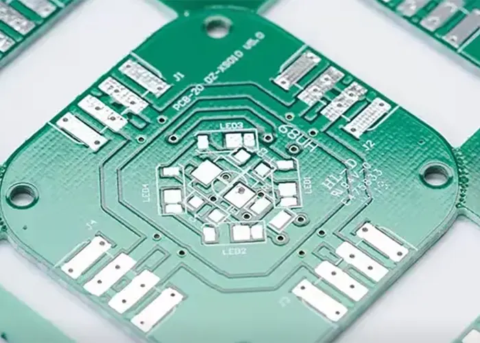
The screenshot below shows the definitions from the IPC standard:
Dimensional Control
SMD: Solder mask exposure/development accuracy (±20–50 μm)
NSMD: Outer layer etching accuracy (±5–15 μm)
Effective Soldering Area
SMD: Only the copper surface within the solder mask opening (smaller)

NSMD: Top and side surfaces of the copper pad (larger)

Typical Applications
SMD: BGA (especially ≥0.5mm pitch), LGA, 01005 passive components, automotive electronics
NSMD: Fine-pitch BGA (<0.5mm), high-frequency/high-power applications, scenarios requiring high solder joint strength
Key Design Considerations
Mechanical Reliability vs. Solder Joint Strength
The core advantage of SMD lies in Pad Peel Strength.
Since the copper foil area exceeds the solder mask opening, the solder mask acts as an “anchor” covering the edges of the copper pad, mechanically locking the copper foil to the substrate.
Experimental data shows that the PCB-to-pad bond strength in SMD designs is approximately 53% higher than in NSMD designs (based on pull-out force testing).
This enables superior performance under drop impact, vibration, and thermal cycling conditions, helps reduce the risk of BGA ball cracking, and can even replace certain underfill processes to lower costs.
However, the strength of the solder joint in SMD designs is actually weaker.
This is because the effective solder wetting area is limited to the solder mask opening, and during reflow, thermal expansion of the solder mask may squeeze the solder, reducing the actual soldering area.
In contrast, NSMD allows solder to wrap around the sides of the copper pad, creating a larger IMC (intermetallic compound) contact area, which increases the solder joint’s shear strength by approximately 30%, making it more suitable for high-power or high-thermal-conductivity applications.
High-Density Routing (Escape Routing) Capability
NSMD copper pads can be made smaller (typically 20% smaller than BGA ball diameter), while the solder mask openings are larger, creating critical space for BGA breakout routing.
In ultra-fine-pitch designs with a pitch of 0.4 mm or less, NSMD is virtually the only viable option, as SMD requires a larger copper area to maintain solder mask coverage, which severely constricts routing channels and may even make it impossible to use Dogbone or Via-in-Pad structures.
Thermal Management and Electrical Design
SMD allows for a more complete copper plane beneath the pad (since the solder mask defines the soldering area, eliminating concerns about solder overflow short circuits), which is beneficial for impedance control in power distribution networks and heat dissipation.
However, with NSMD, if connected to thick traces or large copper pads, solder may wick up along the copper surface, altering the actual solder joint geometry. This effect must be mitigated by using symmetrical connections with fine traces (recommended trace width ≤ 100 μm).
Manufacturing Challenges and Process Differences
Cumulative Tolerances and Control Difficulties
⚠️ The critical weakness of SMD lies in the alignment accuracy of the solder mask.
Mechanical positioning errors in the solder mask exposure machine, substrate thermal expansion, and optical distortion typically result in solder mask alignment tolerances of around ±50μm.
Any misalignment will directly alter the effective pad size, causing misalignment between BGA balls and pads, and potentially leading to tombstoning or cold solder joints. The industry requires solder mask alignment tolerances to be controlled within ±1 mil (25.4 μm), but this poses a severe challenge for both equipment and materials.
⚠️NSMD relies more heavily on etching precision.
Modern PCB outer layer etching using LDI (Laser Direct Imaging) can achieve ±5μm precision, and the size of the copper pads is not affected by solder mask misalignment, resulting in better dimensional consistency.
However, NSMD requires that the solder mask openings be uniformly larger than the copper pads (typically ≥1–3 mil on one side). If the solder mask dams are too narrow, the dam structure may not be maintained, increasing the risk of short circuits between adjacent pads.
Surface Treatment and Oxidation Risks
The copper pads in NSMD are fully exposed. If stored for too long after OSP (Organic Solder Mask) treatment, oxidation of the copper surface can lead to reduced solderability;
In contrast, the copper edges of SMD pads are covered by the solder mask, with only the center of the opening exposed. This results in a smaller oxidized area and higher tolerance to storage and reflow atmospheres.
Special Processes: Via-in-Pad and Via Filling
For vias beneath SMD pads, resin plugging combined with electroplating (Filled & Capped Via) must be used; otherwise, solder will be drawn into the holes during reflow (solder wicking), causing sunken joints or voids.
In contrast, NSMD pads can offset the via using a “dogbone” structure, reducing reliance on the via-filling process—a key advantage in cost-sensitive designs.
Process Differences at the Component Placement Stage
Solder Paste Printing (Stencil Printing)
SMD offers significant advantages during the printing process. After the solder mask covers the edges of the copper pads, it forms a “wall” slightly higher than the copper surface.
When the stencil is pressed against the board, it adheres tightly to the solder mask, creating a better gasketing effect and reducing the risk of solder paste overflowing from the bottom of the stencil.
This results in higher solder paste transfer efficiency and more consistent solder paste volume, which is critical for ultra-small passive components such as 01005 and 0201, as well as 0.3mm pitch CSPs.
NSMD presents even greater printing challenges. Since the copper pad is lower than the solder mask (typically 20–30 μm thick), a tiny gap exists between the stencil and the copper surface, which can easily lead to uneven solder paste deposition or “dog-ear” defects.
Furthermore, even a slight misalignment between the stencil apertures and the copper pads can cause solder paste to land in the solder mask area, resulting in random solder balls.
Component Placement
SMD solder mask apertures are regular in size and unaffected by copper etching deviations, providing a more stable reference for vision systems and helping to improve placement accuracy for fine-pitch BGAs.
In contrast, NSMD pads may exhibit asymmetrical shapes due to uneven etching or the influence of trace connections.
This can result in uneven deflection forces during component “self-alignment,” increasing the risk of placement misalignment.
Reflow Soldering and Defect Patterns
1️⃣ Solder Bridging
SMD: Lower risk (solder mask barriers restrict solder flow)
NSMD: Higher risk (especially without solder mask barriers)
2️⃣ Voids
SMD: Higher risk (solder mask coverage restricts gas escape)
Lower risk for NSMD (copper pads facilitate gas escape)
3️⃣ Tombstoning/Misalignment
Moderate risk for SMD (misalignment causes uneven stress distribution)
High risk for NSMD (uneven solder volume or asymmetrical copper surfaces)
4️⃣ Pad Lifting
Extremely low risk for SMD (solder mask provides mechanical anchorage)
NSMD: High risk (thermal stress or during rework)

⚠️ During reflow, the CTE difference between the SMD solder mask and the copper/tin layers is significant, potentially generating Z-axis stress.
Under long-term thermal cycling, this can actually increase the risk of cracking at the bottom of the solder joint.
In contrast, NSMD solder joints are more flexible and have a more uniform stress distribution, typically offering superior thermal fatigue life compared to SMD.
Conclusion
The choice between SMD and NSMD is fundamentally a trade-off between “mechanical anchoring strength” and “electrical performance/solder joint integrity.”
SMD enhances the survival of pads on the PCB substrate through mechanical locking by the solder mask, making it suitable for high-stress environments;
NSMD, on the other hand, optimizes electrical connectivity and high-density routing capabilities by maximizing the exposed copper area and solder wetting range.
Contemporary high-end design trends favor a scenario-based, hybrid approach rather than a one-size-fits-all solution.
This requires designers to have a deep understanding of the manufacturing capabilities of PCB manufacturers (such as solder mask alignment accuracy, etching tolerances, and via filling capabilities) as well as the printing and reflow characteristics of assembly facilities in order to make optimal decisions.