PCB defect detection is a critical process in modern electronics manufacturing, ensuring the reliability and performance of printed circuit boards (PCBs), which serve as the core medium for signal transmission and component mounting in electronic devices.
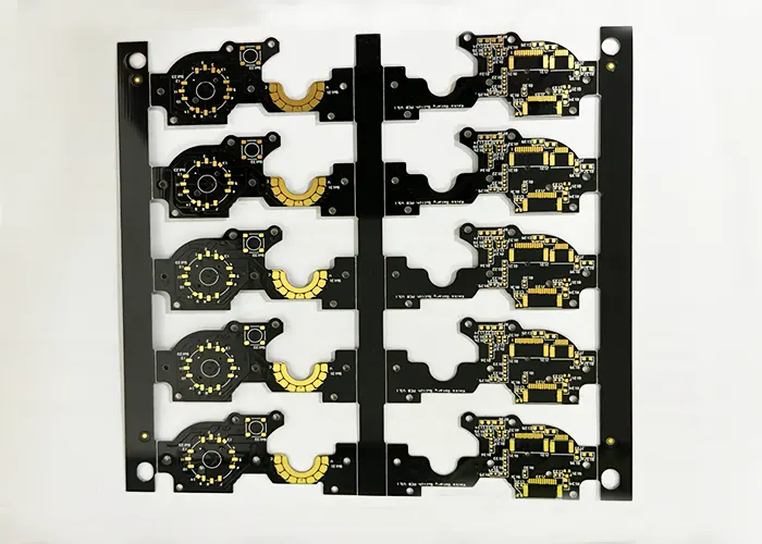
PCBs are widely applied across key industries, including consumer electronics, industrial control systems, automotive electronics, communication networks, as well as computers and servers (see Figure 1).

With the rapid advancement of the electronics and information technology sectors, PCB designs are becoming increasingly complex, characterized by higher circuit density and greater integration levels.
As a result, the demand for accurate, efficient, and scalable PCB defect detection methods continues to grow, playing a vital role in maintaining product quality and supporting the evolution of high-performance electronic systems.
Printed Circuit Board Testing
Printed circuit board testing plays a critical role in ensuring the performance and reliability of modern electronic products.
As electronic systems become increasingly complex and compact, effective testing methods are essential for identifying defects early and maintaining consistent product quality across the entire manufacturing lifecycle.
The Importance of Printed Circuit Board Testing
As an indispensable fundamental component in electronic devices, the quality of printed circuit boards directly determines the reliability, stability, and service life of the entire system.
Therefore, conducting precise and efficient fault detection holds significant engineering importance.
However, during design, manufacturing, and assembly, factors such as process deviations, material defects, or environmental interference often lead to various types of failures, including open circuits, short circuits, and cold solder joints.
The impact of such failures is particularly significant in high-reliability applications such as consumer electronics, industrial automation, automotive electronics, and aerospace.
For example:
- A micro-short circuit on a smartphone’s motherboard may prevent the device from booting;
- Poor solder joints on industrial robot control boards can cause sudden interruptions in production lines;
- Open-circuit faults in printed circuit boards within new energy vehicle battery management systems may pose driving safety hazards;
- In aerospace equipment, the failure of any single printed circuit board can directly impact the flight safety and mission reliability of the entire system.
PCB Inspection Methods Must Keep Pace with the Times
As modern electronic devices continue to evolve toward miniaturization and higher performance, the integration density of printed circuit boards (PCBs) is increasing, with circuit line spacing gradually shrinking to the micrometer level.
Against this backdrop, traditional PCB fault detection methods are increasingly revealing limitations such as insufficient efficiency and high false-negative rates, making it difficult to meet the dual demands of detection accuracy and efficiency in current industrial manufacturing.
Therefore, researching and developing high-precision, high-efficiency methods for identifying and detecting PCB defects is of great significance for improving electronic product quality and advancing production automation.
In recent years, artificial intelligence technologies, particularly deep learning, have achieved breakthroughs in various computer vision tasks—such as image classification and object localization—due to their significant advantages in automatic feature extraction and complex pattern recognition.
This has provided a new technical pathway for addressing the automatic detection of microscopic defects on PCBs.
Principles of Deep Learning and Machine Vision
Deep learning and machine vision provide the foundational technologies for modern automated inspection systems.
By enabling machines to interpret visual data with high accuracy, these technologies play a crucial role in detecting complex patterns and microscopic defects in industrial applications such as printed circuit board inspection.
Convolutional Neural Networks and Image Recognition
As a key branch of machine learning, deep learning is fundamentally based on artificial neural networks.
By constructing network structures comprising multiple hidden layers, it achieves high-level abstraction and hierarchical feature representation of input data.
The core idea of deep learning lies in simulating the mechanisms of information transmission and processing in biological neural systems.
By leveraging large-scale datasets to iteratively optimize parameters such as weights and biases within the network, the model can automatically learn complex underlying patterns from raw data, rather than relying on expert experience or manually designed feature extractors.
This “end-to-end” learning paradigm has demonstrated significant advantages in numerous fields.
In image recognition tasks, convolutional neural networks (CNNs) are among the most widely used and effective deep learning models.
Their typical architecture consists primarily of convolutional layers, pooling layers, activation function layers, and fully connected layers.
Convolutional layers use learnable convolutional kernels to perform local sliding computations on the input image, effectively extracting spatial features such as edges, corners, and texture information;
Pooling layers typically employ max-pooling or average-pooling operations to downsample the feature maps produced by the convolutional layers, reducing the number of parameters while preserving key features, thereby enhancing the model’s computational efficiency and generalization ability;
The introduction of activation functions endows the network with nonlinear transformation capabilities, enabling the model to capture complex feature mapping relationships;
Finally, the fully connected layer is responsible for mapping the feature vectors, which have undergone multiple levels of abstraction, to the sample label space, thereby completing the final classification decision.
Currently, representative convolutional neural network architectures include the early LeNet, as well as subsequent developments such as AlexNet, VGGNet, and InceptionV3, which have continuously advanced the frontiers of image recognition technology in terms of structural design and performance.
Capsule Networks and Printed Circuit Board Inspection
Capsule Networks (CapsNet) use “capsules” as their basic computational units, with each capsule represented as a vector composed of a group of neurons.
The magnitude of this vector is typically used to represent the probability of a specific feature’s presence, while the direction of the vector encodes the feature’s internal pose parameters, such as specific attributes like position, rotation, and scale.
Compared to traditional convolutional neural networks, where neuron outputs are scalar values, CapsNet preserves richer feature information through vectorized outputs, thereby offering greater expressive power when representing objects.
CapsNet employs a dynamic routing mechanism to facilitate information transmission and interaction between different capsule layers.
Through an iterative process, the algorithm determines the coupling coefficients between lower-level and higher-level capsules, enabling the network to autonomously learn the spatial hierarchical relationships between parts and the whole.
Consequently, capsule networks can effectively capture complex spatial relationships among features in images—such as the relative positions of components, angular variations, and dimensional scaling—thereby achieving a more comprehensive and robust representation of the target.
Compared to widely used convolutional neural networks, capsule networks demonstrate significant advantages in multiple aspects.
First, their vector-form outputs not only indicate whether a feature is present but also characterize various internal attributes of that feature, thereby providing richer feature information than scalar activation values.
Second, the dynamic routing mechanism enables the model to autonomously learn part-whole relationships among features without relying on extensive spatial invariance prior knowledge, resulting in stronger recognition robustness when processing objects that undergo deformation, rotation, or partial occlusion.
Furthermore, capsule networks are highly sensitive to subtle structural changes in the input, enabling them to effectively detect minute anomalous features that are easily overlooked by the human eye or traditional models.
This characteristic makes them particularly well-suited for high-precision PCB defect detection on printed circuit boards, which feature diverse defect morphologies and minute dimensions.
Consequently, leveraging its unique vectorized feature representation, spatial relationship modeling capabilities enabled by dynamic routing, and high sensitivity to subtle features, the Capsule Network demonstrates potential performance advantages in PCB defect detection tasks.
It is expected to achieve more accurate and stable recognition results in complex industrial quality inspection scenarios.
Experimental Design and Analysis
This section outlines the experimental framework used to evaluate the effectiveness of different deep learning models for printed circuit board defect detection.
It covers dataset preparation, model configuration, and performance evaluation to ensure objective and reproducible results.
Raw Image Data Processing
A publicly available printed circuit board defect dataset was used as the experimental data source.
This dataset covers six common types of PCB defects, specifically including missed vias, short circuits, open circuits, burrs, rat bites, and excess copper, comprising a total of 693 raw images.
To enhance the model’s generalization ability and mitigate overfitting, this study performed various preprocessing and data augmentation operations on the raw data, including random cropping, rotation, and flipping, expanding the total dataset to 10,668 images.
Examples of defects after data augmentation are shown in Figure 2.

The augmented dataset was divided proportionally into training and testing sets, with 80% used for model training and the remaining 20% serving as the testing set to evaluate model performance.
Experimental Methodology
Given the characteristics of the printed circuit board fault detection task, this study selected four classic convolutional neural network architectures—LeNet, AlexNet, VGGNet, and Inception V3—and conducted comparative experiments with capsule networks.
All networks were trained using the aforementioned dataset under identical conditions, with the number of training epochs uniformly set to 50 to ensure comparability and consistency across experiments.
The experimental hardware platform consisted of an Intel 10th Gen Core X-series 10-core desktop processor paired with an NVIDIA RTX 20-series graphics card to accelerate the neural network training process.
The operating system was Ubuntu 18.04.5, and all experiments were conducted in this stable environment to ensure the reproducibility of results.
Quantitative tests were conducted on the detection performance of the five models. The results of the metric comparison show:
- For the LeNet training network, the training accuracy, test accuracy, training loss, and test loss were 98.7%, 98.4%, 0.08%, and 0.28%, respectively;
- For the AlexNet model, the training accuracy, test accuracy, training loss, and test loss were 99.49%, 99.58%, 0.26%, and 0.46%, respectively;
- For the VGGNet model, the training accuracy, test accuracy, training loss, and test loss were 99.0%, 98.9%, 0.16%, and 0.26%, respectively;
- The training accuracy, test accuracy, training loss, and test loss of the Inception V3 network are 97.6%, 97.4%, 0.23%, and 0.53%, respectively;
- The training accuracy, test accuracy, training loss, and test loss of the CapsNet network are 99.7%, 99.3%, 68.2%, and 68.4%, respectively.
Recognition and Classification Analysis
Further fault recognition and classification were performed on AlexNet and CapsNet, which achieved higher test accuracies.
The results show:
- Under a short-circuit fault, the recognition accuracies of CapsNet and AlexNet were 99.9897% and 99.9907%, respectively;
- For short-circuit faults, the recognition accuracies of CapsNet and AlexNet were 99.8548% and 99.6472%, respectively;
- For open-circuit faults, the recognition accuracies of CapsNet and AlexNet were 99.9364% and 99.6303%, respectively;
- Under glitch faults, the recognition accuracies of CapsNet and AlexNet were 99.9580% and 99.6465%, respectively;
- Under rodent-bite faults, the recognition accuracies of CapsNet and AlexNet were 99.8628% and 99.8749%, respectively;
- Under excess copper faults, the recognition accuracies of CapsNet and AlexNet were 99.8961% and 99.6125%, respectively.
A comparison reveals that CapsNet achieved recognition accuracies above 99.8% for all six types of printed circuit board faults, outperforming AlexNet.
Further testing under the same experimental conditions yielded the following results:
- When the number of iterations was 1, CapsNet’s training accuracy and test accuracy were 96.3% and 96.5%, respectively;
- When the number of iterations was 2, CapsNet’s training accuracy and test accuracy were 98.3% and 98.1%, respectively;
- When the number of iterations is 3, CapsNet’s training accuracy and test accuracy are 99.7% and 99.3%, respectively;
- When the number of iterations is 4, CapsNet’s training accuracy and test accuracy are 99.1% and 98.7%, respectively;
- When the number of iterations is 5, CapsNet’s training accuracy and test accuracy are 99.0% and 98.5%, respectively;
- When the number of iterations is 6, CapsNet’s training accuracy and test accuracy are 98.1% and 96.4%, respectively.
A comparison reveals that when the number of iterations is 3, CapsNet achieves the best fault identification classification performance and the highest accuracy.
The accuracy of the CapsNet under different learning rates is shown in Figure 3.

- When the learning rate is 0.01, the accuracy fluctuates as the number of epochs increases, with the most significant fluctuations occurring at 14 epochs;
- When the learning rate is 0.001, the CapsNet accuracy curve converges the fastest and achieves the highest accuracy as the number of epochs increases;
- When the learning rate is 0.0001, the accuracy curve exhibits slight fluctuations as the number of epochs increases, and the convergence rate is slow.
Conclusion
This study focuses on deep learning-based methods for PCB defect detection, with a particular emphasis on comparing the performance of LeNet, AlexNet, VGGNet, Inception V3, and Capsule Networks under identical experimental conditions.
The experimental results show that AlexNet performs exceptionally well in identifying six common types of PCB defects, achieving an accuracy rate of over 99.6%;
whereas the Capsule Network achieved even better recognition results across all defect types, with accuracy rates exceeding 99.8%, demonstrating higher classification accuracy and robustness.
Under the same experimental conditions, the Capsule Network achieved optimal classification performance after just 3 iterations, demonstrating fast convergence and significantly superior recognition performance compared to other benchmark models.
These results indicate that the Capsule Network possesses strong representational capabilities in handling limited samples and subtle defect features, making it more suitable for practical printed circuit board quality inspection scenarios.