Flexible printed circuit boards (FPCBs) are widely used in smartphones, flexible displays, wearable devices, and other fields due to their excellent flexibility and heat dissipation capabilities.
As circuit density continues to increase, the types of surface defects are becoming increasingly complex.
Common defects include short circuits, open circuits, blisters, white spots, black spots, and holes.
Limitations of Traditional Visual Inspection
In traditional inspection methods, RGB image-based template matching is widely used.
This method locates abnormal areas by comparing a reference image with the image under test.
However, such methods are highly sensitive to lighting conditions; when lighting is uneven, false positives or false negatives are likely to occur.
Furthermore, some defects resemble normal circuit structures in appearance, making it difficult to distinguish them accurately using visible light images alone.
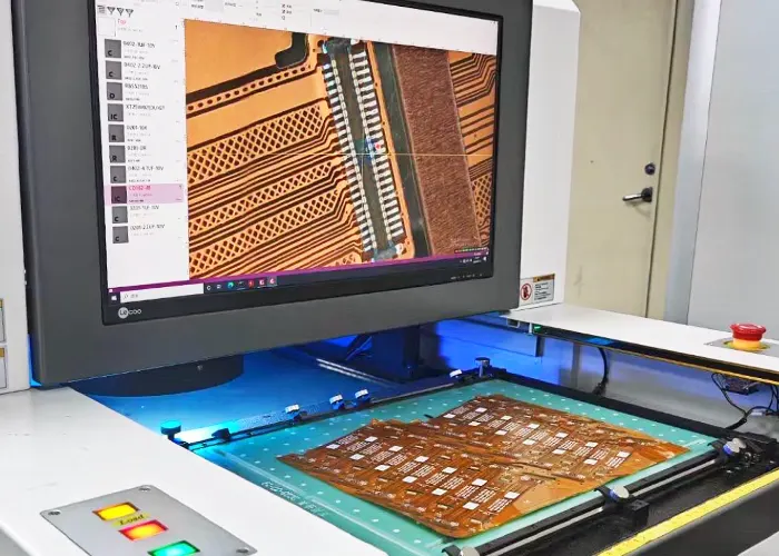
 HSMIsystem. (b) RGB image of an FPCB sample fromthe production line")
Construction of a Hyperspectral Imaging System
To enhance the stability of the detection process, this study developed a hyperspectral microscopic imaging system.
The system consists of a hyperspectral camera, a microscope, and data acquisition software.
The hyperspectral camera used is the FS-23 model from Caispect Technology, which has a spectral range of 400–1000 nm and a spectral resolution of 2.5 nm.
The camera uses line-scan imaging, and the raw data contains 1,200 spectral bands.
To facilitate processing, the study merged every four adjacent bands into one, resulting in a data structure of 300 bands.
Each hyperspectral image has a resolution of 1,920 × 960 pixels × 300 bands, covering the complete spectral information of the copper conductor and polyimide substrate.
The advantage of hyperspectral imaging lies in its ability to capture continuous spectral curves for each pixel.
The study found that the spectral responses of copper and polyimide exhibit significant differences in the 500–750 nm wavelength range, providing a reliable basis for subsequent image segmentation and material identification.

Spectral Information-Driven Detection Method
The detection framework proposed in this study consists of two sub-networks: FPCB-LocNet for defect localization and FPCB-ClaNet for defect classification.
During the localization stage, FPCB-LocNet employs multi-scale 3D convolutional kernels to simultaneously extract features from both the spatial and spectral dimensions.
The network uses two convolution kernels of different sizes, focusing on local spatial structures and spectral features, respectively, and fuses features from different scales via a residual structure.
This design enables the network to simultaneously capture fine spatial textures and continuous spectral variations, achieving pixel-level segmentation of copper and polyimide.
After segmentation, abnormal regions are localized through template matching.
During the classification stage, given the limited number of hyperspectral samples, the network employs a transfer learning strategy: it is first pre-trained on an RGB image dataset of FPCBs and then fine-tuned on false-color images.
To address the issue of class imbalance, the network incorporates class-balanced sampling and weight decay strategies, enabling the model to focus more on defect types with fewer samples.
Additionally, an SE attention mechanism is incorporated to enhance the network’s focus on key features.

Experimental Results and Practical Applications
In terms of image segmentation, FPCB-LocNet outperforms traditional segmentation methods such as the maximum entropy method, the watershed algorithm, and Otsu’s method when processing images with uneven lighting, achieving a segmentation accuracy of 97.86%.
In classification tasks, FPCB-ClaNet achieves a comprehensive classification accuracy of 97.84% for six common defect categories.


Ablation experiments validated the actual contributions of each module: data augmentation improved classification accuracy, while class-balanced sampling and weight decay effectively enhanced the recognition performance for tail classes, and the SE attention mechanism delivered a stable improvement in classification performance with only a small increase in parameters.
The visualization results from Grad-CAM heatmaps indicate that the model’s attention regions align highly with the actual defect locations.
This study combines hyperspectral imaging with deep learning to construct a complete processing pipeline spanning data acquisition, image segmentation, defect localization, and defect classification.
The method can reliably perform FPCB surface defect recognition without relying on specific lighting conditions, providing a viable technical approach for quality management in the manufacturing of high-density flexible printed circuit boards.
Conclusion
This study demonstrates the effectiveness of combining hyperspectral imaging with deep learning techniques for the precise detection of surface defects in FPCB manufacturing.