With the advancement of high-performance electronic devices, the demands placed on printed circuit boards (PCBs) are becoming increasingly stringent.
Among these, thermal management technology has emerged as a hot topic.
This article compiles and organizes relevant information for your reference.
Concept and Significance of Thermal Management
Concept of Thermal Management
Thermal management, as the name suggests, involves managing and controlling the heat generated by electronic devices.
Thermal management technology refers to methods that regulate and control the temperature or temperature difference of a specific object using heating or cooling techniques, based on its specific requirements.
Heat management is reflected in temperature behavior and involves techniques for transferring excess heat from one location to another, driven by temperature differences.
During operation, electronic devices generate heat on the PCB.
It is necessary to find ways to remove excess heat from the PCB and its components to lower their temperatures;
This also falls under the scope of thermal management.
Sources and Transfer of Heat
According to the principles of thermodynamics, heat results from the collision and transfer of microscopic particles within a substance, including the energy generated by the movement, rotation, and vibration of molecules, atoms, and electrons.
In electronic devices, the primary cause of heat generation is the conversion or dissipation of electrical energy into thermal energy (heat) when electronic components perform work under the influence of voltage or current.
This is particularly true for active components such as transistors and integrated circuits during operation.
Secondly, when high power or high current flows through conductors, connectors, or switches, resistance (electrical resistance) is present during the conduction process, resulting in power loss and the generation of heat.
This includes heat generated by PCB copper traces and through-holes due to their inherent resistance; the higher the current, the greater the heat generated.
Additionally, the operating environment surrounding electronic devices also affects their operating temperature.
With the current trend toward miniaturization of electronic devices, components and PCBs are becoming increasingly dense and highly integrated, leading to higher power consumption and, consequently, greater heat generation.
Modes of Heat Transfer
There are three modes of heat transfer: conduction, convection, and radiation.
Conduction refers to the transfer of heat through direct contact between objects, such as heat pipes and heat sinks;
Convection refers to the transfer of heat through the movement of air, such as fan-based cooling;
Radiation refers to the transfer of thermal energy through the emission of electromagnetic waves without the need for a medium, such as infrared radiation.
Conventional Thermal Management Solutions in Electronic Devices
The standard thermal management solutions for electronic devices typically involve convection and conduction, specifically using heat sinks (heatsinks, heat pipes) to provide a path for heat dissipation; and increasing airflow by using fans to force air movement to carry away heat.
With the ongoing miniaturization of electronic devices and the resulting reduced space between components, it is often impractical to install dedicated cooling fans or heat sinks.
Therefore, utilizing the thermal conductivity of the PCB itself may be the most effective thermal management solution.
The Importance of Thermal Management
Thermal management affects the performance, stability, and lifespan of electronic devices.
If electronic components operate at excessively high temperatures without adequate heat dissipation, their performance parameters may change, leading to signal distortion or attenuation, which in turn causes device instability or even failure.
Heat accumulation also accelerates component aging and degradation, thereby shortening the device’s service life.
Any electronic component generates heat when current flows through it.
Up to 50% of failures in electronic devices are caused by excessive temperatures, making thermal management essential to reduce failure rates.
Real-world incidents, such as smartphones catching fire and electric vehicles exploding, are all caused by overheating.
Thermal management requirements were initially driven by high-power communications;
Building on applications in the communications and aerospace sectors, they have rapidly expanded into the automotive, consumer electronics, and medical fields.
Thermal management in the PCB sector has become a critical task, and thermal management technology is one of the fastest-growing segments.
In addition to standard requirements for appearance, dimensions, mechanical and electrical performance, and environmental reliability, modern electronic devices place particular emphasis on signal integrity, power integrity, and thermal management.
Deficiencies in signal integrity or power integrity can lead to reduced functionality or failure of electronic devices;
Improper thermal management, on the other hand, can result in reduced functionality or failure in mild cases, and in severe cases, cause devices to burn out or even lead to disasters.
The importance of thermal management is self-evident.
Thermal Performance Parameters
Thermal Performance Terminology
Thermal management requires a systematic analysis of heat sources and heat transfer to effectively dissipate thermal energy.
This necessitates an understanding of the thermal properties of different materials, making it important to grasp several key terms.
(1) Thermal Conductivity.
Thermal conductivity is a physical quantity that describes a material’s ability to transfer heat.
It represents the ratio of the amount of heat transferred per unit area per unit time to the temperature gradient.
It is also known as the coefficient of thermal conductivity (CTC).
The symbol for thermal conductivity is λ or k.
› Physical Meaning and Units
It represents the amount of heat transferred per unit time (seconds) and per unit area (square meters) along the direction of the temperature gradient (a temperature change of 1 K per meter) under steady-state heat transfer conditions.
The unit is W/(m·K). The formula for thermal conductivity is as follows:
λ=Q/ (A·dt) (1)
In the equation: Q represents the heat transferred through the object;
A represents the area over which heat is conducted; dt represents the temperature gradient, where dt = (T2 – T1) / h, °C/m;
T2 and T1 are the temperatures at the two locations, respectively; and h is the distance between the two locations (material thickness).
› Physical Definition
Thermal conductivity is defined as follows: If two parallel planes, each with an area of 1 m² and separated by a distance of 1 m, are drawn perpendicular to the direction of heat transfer within an object, and the temperature difference between the two planes is 1 K, then the amount of heat transferred from one plane to the other in 1 second is defined as the thermal conductivity of that material.
› Material Property Characteristics
Thermal conductivity is an intrinsic property of a material and is independent of its shape or dimensions.
This means that as long as the material’s composition remains unchanged, its thermal conductivity will not change.
For example, the thermal conductivity of 1 cm³ of copper is exactly the same as that of 10 m³ of copper.
The higher a material’s thermal conductivity, the faster heat flows and dissipates.
(2) Thermal Resistance.
Thermal resistance is a material’s ability to impede heat flow; it is related to the material’s thermal conductivity, thickness, and area.
The symbol for thermal resistance is Rth, and its unit is K·m²/W.
It reflects the magnitude of heat transfer through a medium or between media, indicating the temperature rise per unit area caused by 1 W of heat.
The thermal conductivity of a given material remains constant, while changing the material’s thickness or area will alter the corresponding thermal resistance value.
The formula for thermal resistance is as follows:
Rth=h/ (λ×A) (2)
When heat flows across the interface between two solid objects in contact, the interface itself presents a significant thermal resistance to the heat flow, known as contact thermal resistance.
It appears that the contact thermal resistance between two objects in good contact depends on the actual area of direct contact (the interface); any gap at the interface reduces the contact area and increases the thermal resistance.
(3) Thermal Impedance.
Thermal impedance measures a material’s ability to resist heat flow; it represents the thermal resistance per unit area of the material.
Similar to thermal resistance, it also reflects the magnitude of heat transfer through a medium or between media.
The value of thermal impedance depends on the material’s thermal conductivity and its thickness; thermal impedance = thickness / thermal conductivity.
The symbol for thermal impedance is Zth, and its unit is K·m/W. It indicates the temperature rise per unit thickness caused by 1 W of heat.
The formula for thermal impedance is as follows:
Zth=h/λ (3)
Zth is a function of thickness; changing the material’s thickness will alter this value. This is not a material property, but an object property.
For example, the thermal resistance of a 1-mm-thick copper sheet differs from that of a 2-mm-thick copper sheet;
However, as long as the thickness remains constant, changing the area of the material will not alter this thermal resistance value.
When selecting the dielectric material for a thermally conductive substrate, it is essential to ensure that the material possesses high thermal conductivity and low thermal resistance while maintaining reliable electrical insulation.
Options for reducing thermal resistance include increasing thermal conductivity and optimizing the object’s geometry (reducing thickness and increasing the contact surface area).
Analogy Between Heat and Electricity
To facilitate understanding of thermal performance, a simple analogy with electricity can be used, as shown in Table 1.
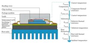
Thermal circuits can be modeled and analyzed by analogy with electrical circuits.
The thermal system configuration and equivalent thermal circuit of a semiconductor device with a heat sink are shown in Figure 1.
This thermal circuit diagram resembles an electrical schematic with resistors connected in series.
In this configuration, the substrate becomes part of the device’s overall thermal design, and the key engineering parameter is the thermal resistance (Rth) of each component.
| Item | Electricity | Heat |
|---|---|---|
| Path | Electrical Circuit | Thermal Circuit |
| Energy | Electrical Energy | Thermal Energy |
| Transfer Capability | Electrical Conductivity σ (S/m) | Thermal Conductivity λ (W/(m·K)) |
| Flow Quantity | Current I | Heat Flow (Temperature) |
| Resistance | Electrical Resistance R | Thermal Resistance Rth |
| Potential | Voltage E (Potential Difference) | Temperature Difference |
| Ohm’s Law | Voltage = Resistance × Current | Temperature = Thermal Resistance × Heat Flow |
| Analogy Formula | R = U/I (V/A) | Rth = T/Q (°C/W) |
| Capacity | Capacitance C | Thermal Capacitance Cth |
| Impedance | Electrical Impedance Z | Thermal Impedance Zth |
Table 1. Analogy Between Heat and Electricity
Thermal Conductivity of Selected Materials
Thermal conductivity is an intrinsic property that characterizes a material’s ability to conduct heat.
Table 2 shows the thermal conductivity (thermal conductivity coefficient) of selected materials.
The microstructure of a material and its energy transfer mechanism determine its ability to conduct heat.
In metals, free electrons dominate heat conduction.
These electrons move rapidly, enabling efficient heat transfer and resulting in high thermal conductivity.
Non-metals rely on phonons (lattice vibration waves) to transfer heat;
When phonons propagate through the lattice, they scatter upon encountering grain boundaries, defects, or impurities, leading to a reduction in thermal conductivity.
Single-crystal materials (such as sapphire and diamond) have highly ordered crystal lattices, resulting in minimal phonon scattering and high thermal conductivity;
In contrast, polycrystalline materials (such as alumina ceramics) have thermal conductivities significantly lower than their single-crystal counterparts because grain boundaries impede phonon movement.
Materials with high density generally exhibit higher thermal conductivity.
The approximate ranges of thermal conductivity for various materials are as follows: metals (50–415), alloys (12–120), insulating materials (0.03–0.17), liquids (0.17–0.7), and gases (0.007–0.170) (units: W/m·K).
| Material | Thermal Conductivity (W·m⁻¹·K⁻¹) | Material | Thermal Conductivity (W·m⁻¹·K⁻¹) |
|---|---|---|---|
| Diamond | 4800–5300 | Water | 0.59 |
| Diamond-like Carbon | 1000–2200 | Air | 0.024–0.027 |
| Silver | 420 | Phenolic Resin | 0.15–0.25 |
| Copper | 390 | Epoxy Resin | 0.20–0.22 |
| Gold | 318 | Polytetrafluoroethylene (PTFE) | 0.20–0.35 |
| Aluminum | 180 | Polyphenylene Oxide (PPO) | 1.0 |
| Silicon | 149 | Polyimide (PI) | 0.10–0.30 |
| Tin | 67 | Polyester (PET) | 0.022 |
| Iron/Steel | 60 | Liquid Crystal Polymer (LCP) | 0.72–0.79 |
| Aluminum Oxide | 30 | Carbon Composite Material | 0.007–0.170 |
| Silicon Nitride | 16.7 | Glass Fiber | 0.032–0.050 |
| Ordinary Ceramics | 0.5–1.5 | FR-4 Glass Fiber Laminate | 0.20–0.25 |
| Glass | 1.1 | CEM-3 Composite Copper-Clad Laminate | 0.40 |
Table 2. Thermal Conductivity of Selected Materials
PCB Thermal Management Design
Basic Approach
First, identify the primary heat sources on the PCB, which include active components, high-power currents, high-frequency signals, and environmental factors.
Engineers first estimate how much heat the circuit will generate during operation.
Based on this understanding, they select an appropriate thermal management solution.
These solutions include optimizing layout design, selecting suitable materials, adjusting copper thickness, utilizing thermal conduction paths, applying metal substrates, and using embedded copper block technology.
PCB layout solutions are the preferred cost-effective method for thermal management.
The basic approach is as follows:
① Establish thermal management awareness early in the design process and consider heat dissipation strategies;
② Distribute heat-generating components and avoid grouping them together, except when they need to share a single heat sink;
③ Allocate ample space for heat-generating components or place them near spacious edges;
④ Keep heat-generating components away from heat-sensitive components;
⑤ Consider wider traces for heat dissipation, potentially using thicker copper foil;
⑥ Implement special PCB structures when necessary.
Conducting thermal simulations early in the design process to evaluate temperature distribution across the entire PCB design—to understand how much heat is generated and where it is located on the board—is a critical step.
We know that the electrical performance of electronic systems is closely related to thermal distribution;
Both resistance and power dissipation affect temperature, and the system’s thermal profile itself depends on electrical performance.
Furthermore, localized high-current surges can create adverse hotspots, leading to thermal runaway and causing serious failures.
Therefore, transient simulation is critical to successful electronic design.
Selecting PCB Thermal Management Solutions
Depending on the heat generation and thermal management requirements of the PCB application, as well as the product’s cost considerations, there are various PCB thermal management solutions available.
This article focuses solely on thermal management measures specific to the PCB itself; external cooling measures are not covered here.
1. Substrate Materials
The simplest solution for PCB thermal management is to directly select substrates with high thermal conductivity, including copper-clad laminates (CCL), prepreg materials (PP), and related insulating media.
Conventional FR-4 and composite epoxy material (CEM-3) laminates have thermal conductivities below 0.5 W/m·K.
While these CCLs are low-cost and easy to process, their thermal conductivity is relatively low.
Consequently, improvements have been made to the existing systems to enhance the thermal conductivity of the substrate.
› Methods for Improving Thermal Conductivity of CCLs
To improve the thermal conductivity of CCLs, one approach is to modify the resin structure—for example, by altering the physical structure of epoxy resin molecular chains to increase polymer crystallinity, thereby enhancing thermal conductivity.
And second, incorporating highly thermally conductive insulating fillers, such as ceramic-based inorganic fillers, into the resin to improve its thermal conductivity through physical blending.
Examples of inorganic fillers include aluminum nitride (AlN), silicon nitride (Si3N4), boron nitride (BN), aluminum oxide (Al2O3), magnesium oxide (MgO), and silicon carbide (SiC).
› Thermal Conductivity Levels and Material Applicability
The applicability of a range of thermally conductive laminate materials is shown in Table 3, which illustrates the impact on cost and availability; as thermal conductivity increases, costs typically rise as well.
| Thermal Conductivity Level | Thermal Conductivity (W·m⁻¹·K⁻¹) | Processability | Cost | Composition and Application Fields |
|---|---|---|---|---|
| Low | 0.2–0.6 | Good | Low | FR-4, general electronic equipment |
| Low+ | 0.7–1.0 | Poor | Medium | Modified epoxy glass cloth multilayer boards, suitable for thick copper and high-voltage applications |
| Medium | 1.2–1.8 | Medium− | Medium+ | Modified epoxy glass fiber systems, suitable for automotive and LED products |
| Medium | 1.0–2.0 | Good | Low | Modified CEM-3, suitable for LED and consumer electronics |
| Medium+ | 2.0–2.4 | Poor | Medium+ | Epoxy glass fiber filled with ceramics, used in power and industrial control multilayer boards |
| Medium+ | 0.8–1.3 | Poor | High | PTFE glass cloth filled with ceramics, suitable for microwave power amplifiers |
| Medium+ | 1.2–1.6 | Medium | High | Carbon fiber reinforced epoxy-filled inorganic materials, suitable for high-frequency high-speed boards |
| High | 20–170 | Poor | High | Ceramic substrates, suitable for high-voltage and high-temperature environments |
Table 3. Thermal Conductivity Suitability of Laminated Substrates
› Development Trends in High-Thermal-Conductivity Substrates
There is a growing demand for thermally conductive substrates capable of operating at higher temperatures.
A new generation of thin laminates and prepregs with high thermal conductivity and high glass transition temperatures is currently under development.
However, resin-based laminates ultimately have limited thermal conductivity.
The use of ceramic substrates represents a promising direction for high-thermal-conductivity substrates.
› Ceramic Substrates for High-Performance Applications
Due to their high heat resistance, excellent thermal conductivity, strong electrical insulation, and dimensional stability, ceramic substrates are used in specialized applications.
Since the thermal conductivity of ceramic materials varies significantly depending on their composition, it is possible to select a ceramic substrate with an appropriate cost-performance ratio based on specific requirements.
In the field of heat dissipation for high-power and high-frequency electronic devices, engineers frequently choose aluminum nitride, silicon nitride, and aluminum oxide.
These materials provide high thermal conductivity, low thermal expansion coefficients, stable performance, and moderate cost.
2. Thermal Surfaces and Thermal Vias
In PCB design, thermal surfaces (heat dissipation surfaces) and thermal vias (heat dissipation vias) are used to increase the thermal conduction pathways, as shown in Figure 2.
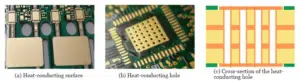
Thermal planes are designed as large copper surfaces, typically utilizing existing power and ground planes.
Designers should strive to transfer heat to the ground plane or mount heat-generating components on the thermal plane to facilitate heat dissipation.
› Function of Thermal Vias and Through-Hole Conduction
Designers place thermal vias beneath surface-mounted heat sources or design them as copper-plated vias that electrically connect to the heat sources, forming an effective thermal conductor between the top and bottom layers of the PCB.
Through-holes conduct both electricity and heat; increasing the thickness of the copper plating inside the through-hole increases heat transfer.
To enhance thermal conductivity, designers fill the holes with conductive and thermally conductive materials to improve both electrical conductivity and heat dissipation.
› Material Thermal Conductivity Performance
The thermal conductivity of non-conductive resin-based fillers is approximately 0.25 W/m·K, while that of conductive silver-copper particle fillers ranges from 3.5 to 10 W/m·K.
The thermal conductivity of electroplated copper exceeds 350 W/m·K.
In comparison, electroplated copper-filled vias offer superior thermal conductivity, equivalent to embedding a fine copper pillar.
Even increasing the thickness of the copper plating in a via by 2.5 μm has a much greater impact on heat transfer than conductive fillers.
› Design Parameters for Thermal Vias
The diameter of a thermally conductive via should be at least 0.30 mm, with a board-to-via diameter ratio (aspect ratio, AR) not exceeding 10.
A larger diameter facilitates complete penetration of the filling material through the via and is also beneficial for copper plating.
Filling through-holes also frees up more space on the PCB surface for component mounting.
› Cost Considerations and Material Compatibility
Utilizing existing ground planes and thermal vias in the design adds almost no cost to the PCB; however, filling the vias increases manufacturing costs.
Another consideration is to match the CTE of the via filler as closely as possible to that of the surrounding laminate material.
3. Thick Copper Conductors
On a PCB, copper conductors carry electrical current; the larger the cross-sectional area of the copper traces, the greater the current they can carry.
Thin traces carrying high currents are prone to overheating and may even burn out.
Therefore, to handle high currents and high power while facilitating heat dissipation, it is necessary to increase the cross-sectional area of the traces.
› Copper Thickness as a Thermal and Electrical Optimization Method
When trace width is limited, increasing the thickness of the copper is a simple method to improve heat dissipation.
For example, when designing a trace width of 100 μm with an allowable temperature rise of 10 °C, a copper foil thickness of 18 μm can handle a current of 1.7 A;
A thickness of 35 μm can handle 4.2 A; and a thickness of 70 μm can handle 6.9 A.
› Heavy Copper PCB Definition and Thickness Range
HCPCBs are defined as boards with a copper layer thickness of 105 μm (3 oz) or greater, including single-sided, double-sided, and multilayer boards.
Generally, the copper layer thickness of HCPCBs ranges from 0.11 to 0.21 mm (approximately 3 to 6 oz); currently, HCPCBs with thicknesses of 0.35 mm (10 oz) and even 0.42 mm (12 oz) are available.
Different copper thicknesses can be selected for different conductor layers within the same printed circuit board.
› Manufacturing Limitations and Line Width Constraints
The copper thickness of the circuit is related to the processing capability for line width and spacing.
It is difficult to process fine circuits on thick copper boards because side etching affects the pattern during etching; see Table 4 for empirical data.
The difference in capability between inner and outer layers lies in the method of copper layer processing.
Inner layers are formed by directly etching copper foil, which ensures good copper foil uniformity;
Outer layers use copper foil combined with electroplated copper to meet the requirements for finished copper, resulting in poor copper foil uniformity.
Keep in mind that the thicker the copper, the more difficult it is to achieve fine lines, and the higher the cost.
There are several process options available for manufacturing thick copper PCBs:
(1) Thick Copper Foil Etching Method:
This method uses a substrate covered with thick copper foil and forms the thick copper circuit pattern through chemical etching.
It applies to the processing of general-purpose thick copper boards.
When the copper layer becomes very thick, the process performs multiple etching passes to reduce side etching of the thick copper.
(2) Copper Plating Thickening Method:
This method thickens the circuit copper layer by performing multiple pattern electroplating passes to achieve the desired thick copper thickness.
Although this process is relatively complex, it can achieve ultra-thick copper layers.
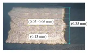
As shown in Figure 3, with a base copper thickness of 0.13 mm, four rounds of pattern electroplating (each with a thickness greater than 0.05 mm) result in a 0.35 mm thick copper circuit.
(4) Thick Copper Semi-Etched Laminating Method:
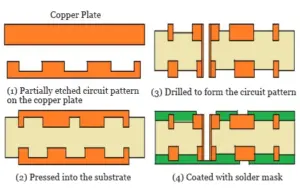
A copper plate of the required thickness undergoes single-sided etching to form the circuit pattern, with the etching depth not penetrating through the plate.
Next, the process presses the patterned side onto the substrate, and fabricates the circuit pattern on the copper plate side to complete the thick copper PCB.
The process is shown in Figure 4.
(5) Cut-and-form Lamination Method:
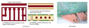
Copper foil of the required thickness is milled or otherwise machined to form the circuit pattern, which is then laminated to the substrate.
Depending on the design requirements, this can serve as an inner or outer layer.
The cut-and-form lamination method is used to manufacture HCPCBs, as shown in Figure 5.
4. Embedded Copper Blocks
5. Metal-Cored (Core) PCBs
Metal has excellent thermal conductivity; attaching a metal plate to one side or the center of a PCB provides effective heat dissipation, effectively acting as a heat sink.
Conclusion
Increasing Importance of Thermal Management
As electronic devices continue to develop toward higher power density, greater integration, miniaturization, and higher operating frequencies, thermal management has become a critical factor affecting PCB performance, reliability, and service life.
Excessive heat can degrade signal integrity and power integrity, accelerate material aging, reduce component reliability, and even cause severe failures such as burnout or fire. Therefore, thermal management is now a core requirement in modern PCB design.
Key Thermal Management Principles
This article reviewed the basic concepts of thermal management, including heat generation, heat transfer modes, and important thermal parameters such as thermal conductivity, thermal resistance, and thermal impedance.
Comparing thermal systems with electrical circuits allows engineers to analyze PCB thermal behavior more intuitively and better understand heat flow and optimize thermal paths.
PCB Thermal Management Solutions
Effective PCB thermal management requires a combination of material selection, structural optimization, and manufacturing technology.
Common solutions include:
- Using high-thermal-conductivity substrate materials
- Designing thermal planes and thermal vias
- Increasing copper thickness and using heavy copper structures
- Embedding copper blocks
- Adopting metal-cored PCBs
Each method provides different advantages in thermal performance, manufacturability, and cost.
Future Development Trends
With the rapid growth of high-power electronics, electric vehicles, 5G communication systems, aerospace equipment, and AI hardware, demand for advanced PCB thermal management technologies will continue to increase.
Future developments will focus on higher thermal conductivity materials, more integrated cooling structures, advanced packaging technologies, and intelligent thermal design methods.
Overall, thermal management will remain one of the most important technologies in modern PCB and electronic manufacturing engineering.