
Printed circuit boards (PCBs) serve as the key medium for signal transmission and circuit connections in electronic devices, and their surface quality directly determines the operational stability of these devices.
Machine Vision-Based PCB Surface Defect Detection
With the rapid development of artificial intelligence, the spacing between PCB traces and the size of via holes have continued to shrink, imposing stricter requirements on the detection of surface defects.
Advances in PCB Defect Detection Algorithms
In recent years, object detection algorithms such as RTDETR, YOLO, and Faster RCNN have opened up new technical pathways for quality control in the PCB manufacturing process.
Proposed Machine Vision-Based Approach
To address the issues in existing methods, this paper proposes a machine vision-based PCB surface defect detection technology.
This technology effectively integrates multiple fields, including image acquisition and image processing, providing robust technical support for quality improvement and intelligent upgrading in the PCB manufacturing industry.
Design of an Intelligent Method for Detecting Surface Defects on PCBs Using Machine Vision
Region-Adaptive Segmentation Based on Machine Vision
Due to the dense circuitry on the surface of printed circuit boards and the gray-level differences between the component mounting areas and the substrate background, this paper first applies a gray-level transformation to the image to further enhance the contrast between the mounting areas and the background.
The linear transformation is shown in Equation (1):

Where: I(x, y) represents the pixel grayscale value of the enhanced output image; f(x, y) represents
the pixel grayscale value of the original input PCB image;
[a, b] represents the grayscale range of the input image;
[c, d] represents the grayscale range of the output image.
The linear grayscale transformation significantly enhances the contrast between the target region and the background in the image.
This enhancement establishes a solid foundation for subsequent precise segmentation.
Binarization for Core Structure Extraction
To further accurately extract core structures such as conductors and pads from the enhanced image, the image must undergo binarization.
Threshold segmentation aims to convert the PCB image into a binary image, thereby extracting core structures such as conductors and pads.
This paper employs the Otsu adaptive thresholding algorithm to achieve this objective.
Let N denote the total number of pixels in the PCB image to be processed; Equation (2) calculates the normalized probability of grayscale values:

In the equation: Pi is the normalized probability of the grayscale value; ni is the number of pixels; N is the total number of pixels in the image.
The Otsu algorithm iterates through all possible thresholds, divides the image pixels into target and background regions, and calculates the inter-class variance between the two regions to determine the optimal segmentation threshold, as shown in Equation (3):

In the equation: σ2 represents the inter-class variance corresponding to the threshold;
w0 represents the proportion of pixels in the target region;
w1 represents the proportion of pixels in the background region;
μ0 represents the average gray-level value of the target region; and μ1 represents the average gray-level value of the background region.
Smoothing Target Regions with Gaussian Filtering
Detecting Edges of PCB Surface Structures
To accurately extract the contour edges of PCB traces and pads, this paper employs the Roberts operator to detect edges, thereby achieving a rough edge localization.
Equation (4) calculates the gradient magnitude:

Where: R(i, j) is the gradient magnitude at the current pixel; fx is the x-coordinate gradient; And fy is the y-coordinate gradient magnitude.
The system sets an adaptive edge threshold and identifies a pixel as an edge point when its gradient magnitude exceeds the threshold. This process produces a preliminary edge contour of the target area on the PCB.
To further improve edge quality, the system applies the Laplace operator for edge enhancement, as shown in Equation (5):

Where: W is the set of enhanced edge pixels; G is the standard deviation of the Gaussian function;
p is the Laplace operator; S is the target defect region;
L(x) is the Laplace function; m is the impulse response window.
This operation effectively enhances edge contrast, providing strong support for the precise extraction of defect regions in subsequent steps.
Intelligent Detection of PCB Surface Defects Based on an Optimized SVM
To address variations in the position and orientation of PCB components, the study employs a rotational adaptive template matching strategy as follows:
The system uses the center of mass of the target contour as the rotation center and the side length of the circumscribing square as the reference, performing a template match every 5° of rotation to cover all possible component orientations.
Equation (6) shows the matching operation:

Where: R(x, y) represents the template matching result; T(i, j) represents the template image; and I'(x, y) represents the region to be matched.
The system sets a matching threshold; if the matching result exceeds the threshold, it considers the match successful and determines that the corresponding region has no positional deviation.
If the matching result falls below the threshold, the system identifies the region as having a positional deviation or defect and performs further defect classification and identification.
SVM Classification for PCB Defects
Finally, a Support Vector Machine (SVM) classification model is constructed to address the issue of non-linearly separable sample features in PCB defect classification.
Its decision function is shown in Equation (7):

In the equation: f(x) represents the output; N is the number of decision functions; α_i is the support vector coefficient;
K is the kernel function parameter; x_i is the support vector; x is the matrix of samples to be predicted; and b is the bias term.
The classification performance of SVM is highly dependent on the selection of the penalty coefficient and kernel function parameters.
Improperly setting parameters can easily cause the model to overfit or underfit, which reduces the accuracy of defect classification.
Optimizing SVM with Sparrow Search Algorithm
The study applies the Sparrow Search algorithm to adaptively optimize the penalty coefficient and kernel parameters.
This algorithm offers advantages such as fast convergence and strong global search capabilities, enabling it to efficiently find the optimal combination within the parameter space.
The study inputs the optimized parameters into the SVM model to build an optimized SVM defect classifier.
This classifier analyzes parameters in the inspection area and outputs defect category information, achieving intelligent detection of PCB surface defects.
Experiment
Experimental Setup
To verify the performance of the proposed intelligent inspection method, this experiment uses assembled PCBs as the inspection objects and establishes a PCB surface defect detection experimental platform.
A high-resolution CCD industrial camera captures the data.
The system transmits data between the camera and the image capture card via a CameraLink high-speed interface, which provides a bandwidth of up to 10 Gbps and enables latency-free image transmission.
Figure 1 presents the block diagram of the PCB inspection system.
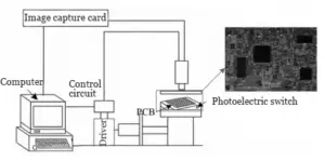
The PCB used in the experiment was a double-sided FR-4 board with a minimum trace spacing of 0.15 mm and pad diameters ranging from 0.2 to 0.8 mm.
| Parameter | Configuration |
|---|---|
| Resolution | 2,448 × 2,048 |
| Frame Rate (FPS) | 60 |
| Lens Focal Length (mm) | 59.9 |
| Random Scaling Ratio | 0.5 |
| Color Space Jitter (%) | ±20 |
| Data Interface | Cameralink |
| Operating Temperature (°C) | −30 ~ 50 |
Table 1. Machine Vision Parameter Configuration
Random scaling and color space perturbation operations simulated the variability found in real-world environments during the data preprocessing stage, enhancing the model’s generalization ability.
A defect sample database captured common defect types on PCB surfaces to comprehensively evaluate the proposed method’s performance in detecting different types of defects.
This database includes five categories of defects: notches, pitting, foreign objects, abnormal protrusions, and short circuits.
For each category, the study selected 100 high-quality images for the test set, totaling 500 images, to evaluate the performance of the proposed method.
Analysis of Image Registration Results
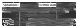
Statistical analysis shows that, for a single PCB image, the proposed method can extract 1,283 stable feature points, thereby eliminating detection errors caused by deviations in the PCB’s orientation.
Visualization of Defect Detection Results
To verify the practical effectiveness of the proposed method, the study conducted defect detection experiments using PCB images from the test set. Figure 3 shows the results.
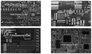
And for circuit break defects, the detection confidence reaches 98.7%.
The experimental results fully demonstrate the capability of the proposed method to detect various types of surface defects.
The method also shows excellent practical applicability.
Comparison of Surface Defects
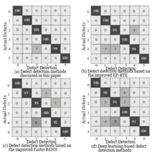
To further evaluate the performance of the proposed detection method, the study used a confusion matrix to compare it with three other methods.
Figure 4 shows the detection results for the five defect categories using the different methods.
Figure 4 shows that the proposed detection method identifies various surface defects on PCBs by integrating adaptive image preprocessing, registration, and an optimized classifier.
The proposed method achieves a detection accuracy of 99.8%.
The three comparison methods achieve detection accuracies of 98.1%, 98%, and 96.5%, respectively, all of which fall below the accuracy of the proposed method.
The results indicate that the proposed detection method satisfies the accuracy and real-time requirements for PCB surface defect detection.
The method also demonstrates high engineering application value.
Conclusion
The proposed intelligent defect detection method uses image segmentation and edge enhancement techniques to accurately extract target regions from complex circuit backgrounds.
This approach effectively improves the accuracy of defect localization.
The method then applies a rotational adaptive template matching algorithm and combines it with an SVM classifier optimized using the Sparrow Search algorithm, successfully detecting surface defects on PCBs.
Experimental results demonstrate that the method achieves a 99.8% accuracy rate in detecting common defects in PCBs, providing an effective technical solution for intelligent inspection in the PCB manufacturing industry.