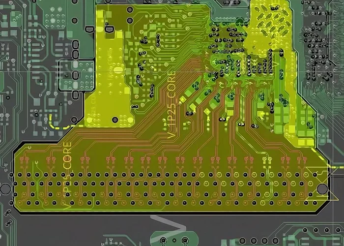
With the rapid development of high-speed electronic systems, signal integrity has become a core concern in modern PCB design.
High-speed differential signal routing, impedance matching, grounding design and anti-interference measures directly determine the stability and performance of circuits.
This document collects common practical problems encountered in high-speed cabling, including differential pair layout, impedance parameter setting, grounding copper design, signal line matching and conflicts between theoretical rules and actual layout.
Combined with professional electromagnetic and circuit theory, targeted analysis and solutions are provided for these typical issues.
About High-Speed Differential Signal Routing
Questions:
When routing high-speed differential signal pairs close together and parallel on a PCB, provided impedance matching is achieved, mutual coupling between the two lines can offer many benefits.
However, some argue that this increases signal attenuation and affects transmission distance.
Is this true, and why? On evaluation boards from some large companies, I’ve noticed that in high-speed routing, some designs place the lines as close together and parallel as possible, while others intentionally vary the distance between them.
I’m unsure which approach yields better results. Our product’s signal operates at around 1 GHz with a 50-ohm impedance requirement.
When performing software calculations, should the differential pair be modeled at 50 ohms or 100 ohms?
Is it possible to add a matching resistor between the differential pairs at the receiving end? Thank you!
Answer:
The primary causes of high-frequency signal attenuation are conductor loss (including the skin effect) and dielectric loss.
When analyzing transmission line effects in electromagnetic theory, the extent of their impact on signal attenuation can be observed.
Coupling between differential pairs affects their characteristic impedance, reducing it.
According to the voltage divider principle, this results in a slightly lower voltage being delivered from the signal source to the lines.
As for the theoretical analysis of signal attenuation caused by coupling,
I have not come across any such studies, so I cannot comment on that. When routing differential pairs, they should be kept appropriately close together and parallel.
“Appropriately close” refers to the fact that the spacing between them affects the differential impedance value, which is a critical parameter in differential pair design.
They must also be parallel to maintain consistency in differential impedance.
If the two lines are sometimes close and sometimes far apart, the differential impedance will be inconsistent, which will affect SI and timing delay.
The differential impedance is calculated as 2(Z11 – Z12), where Z11 is the characteristic impedance of the trace itself, and Z12 is the impedance generated between the two differential lines due to coupling, which is related to the line spacing.
As for whether to calculate the differential impedance as 50 ohms or 100 ohms, the answer is actually quite simple: it mainly depends on the requirements of your bus or design platform.
For example, USB 2.0 typically requires an impedance of 90 ohms, while SATA requires 100 ohms; Intel’s X86 motherboards have slightly different requirements.
Therefore, this must be determined based on the specific circumstances.
As for how to calculate this, you can use simulation software. The most commonly used tool is Polar SI9000.

Improving Immunity to Interference
Questions:
To improve immunity to interference, aside from separating the analog and digital grounds and connecting them only at a single point on the power supply, as well as using thicker ground and power lines, I would appreciate some expert advice and suggestions!
Answer:
In addition to isolating the grounds, you should also pay attention to the power supply for the analog circuitry.
If it shares a power supply with the digital circuitry, it is best to add a filter circuit.
Furthermore, digital and analog signals should not cross paths, especially not across ground isolation zones (moats).

Regarding Grounding of Copper Plating in Blank Areas on Signal Layers in High-Speed PCB Design
Question:
In high-speed PCB design, copper plating can be applied to blank areas on signal layers.
Should the copper plating on all signal layers be grounded, or is it better to ground half and connect the other half to the power supply?
Answer:
In most cases, copper plating in blank areas is grounded.
However, when plating copper adjacent to high-speed signal lines, care must be taken to maintain an appropriate distance between the plated copper and the signal lines, as the plated copper can slightly reduce the characteristic impedance of the traces.
Care must also be taken not to affect the characteristic impedance of other layers, such as in stripline structures.
Matching Issues for High-Speed Signal Lines
Question:
In high-speed PCB layout, why is it necessary to match high-speed signal lines (such as CPU data and address lines)? What risks arise if they are not matched?
What factors determine the acceptable length range (i.e., the signal line delay difference), and how is it calculated?
Answer:
The primary reason for requiring matched characteristic impedance in signal lines is to prevent reflections caused by transmission line effects from affecting signal integrity (SI) and propagation time.
In other words, if the lines are not matched, reflections will occur, degrading signal quality.
The length range for all traces is determined based on timing requirements.
Many factors influence signal propagation delay, and trace length is just one of them.
The required length range for certain signal lines is derived from the timing margin calculated under the signal’s transmission mode (common clock or source-synchronous), after which the allowable tolerance for trace length is established.
About signal integrity issues
Question:
In high-speed design, how can signal integrity issues be addressed?
Answer:
Signal integrity is essentially a matter of impedance matching.
Factors affecting impedance matching include the signal source architecture and output impedance, the characteristic impedance of the traces, the characteristics of the load, and the topology.
The solution involves termination and adjusting the trace topology.
How to Address Theoretical Conflicts in Practical PCB Layout
Question:
In practical PCB layout, many theoretical principles conflict with one another.
For example: a) Connecting multiple analog and digital grounds: In theory, they should be isolated from one another.
However, in actual miniaturized, high-density layouts, space constraints or the need for absolute isolation can result in excessively long traces for small-signal analog ground, making it difficult to implement the theoretical approach.
My approach is to isolate the analog and digital ground planes of a functional module into a complete, self-contained island, with all analog and digital grounds for that module connected to this island.
I then use a ground channel to connect the island to the “main” ground.
I’m not sure if this approach is correct. b. In theory, the connection between the crystal oscillator and the CPU should be as short as possible.
However, due to layout constraints, the connection is relatively long and thin, leading to interference and unstable operation.
How can this issue be resolved through routing? There are many similar issues, especially when considering EMC and EMI in high-speed PCB routing, which often result in conflicts and are quite challenging.
How can these conflicts be resolved? Thank you!
Answer:
a. Basically, isolating the analog and digital grounds is the correct approach.
It is important to ensure that signal traces do not cross the isolation area (moat) whenever possible, and to avoid creating excessively long returning current paths for power and signals.
b. A crystal oscillator is an analog positive-feedback oscillation circuit.
To maintain a stable oscillation signal, it must meet specifications for loop gain and phase.
However, these analog oscillation specifications are easily susceptible to interference, and even adding ground guard traces may not fully isolate the interference.
Furthermore, if the distance is too great, noise on the ground plane can also affect the positive-feedback oscillation circuit.
Therefore, it is essential to place the crystal oscillator as close as possible to the chip.
c. It is true that high-speed routing and EMI requirements often conflict.
However, the fundamental principle is that resistors, capacitors, or ferrite beads added to mitigate EMI must not cause the signal’s electrical characteristics to deviate from specifications.
Therefore, it is best to first address or minimize EMI issues through routing techniques and PCB stackup design—such as routing high-speed signals on inner layers—and only use resistors, capacitors, or ferrite beads as a last resort to minimize signal degradation.
Conclusion
In high-speed PCB design, reasonable routing, accurate impedance control and standardized grounding are the keys to ensuring signal integrity.
Differential pairs should be laid out in parallel with uniform spacing to stabilize differential impedance.
The value of differential impedance must comply with the specifications of the actual bus protocol.
Proper ground isolation and copper laying rules effectively enhance anti-interference capability.
In practical layout, designers need to flexibly balance theoretical principles and space constraints, prioritizing routing optimization to address EMC and EMI issues before incorporating auxiliary components.
Following the above design guidelines can effectively reduce signal reflection, attenuation and interference, and guarantee reliable operation of high-speed circuits.