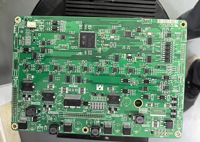
Surface-Mount Technology (SMT) is often introduced as a method for attaching components to printed circuit boards (PCBs), but this definition barely scratches the surface.
In reality, SMT serves as the backbone of modern electronics manufacturing, enabling miniaturization, high-speed production, and cost-effective system integration.
Over 90% of today’s consumer and industrial electronics—from smartphones to automotive ECUs—rely on SMT, making it far more than a simple assembly method.
Where many articles focus on superficial process steps, they overlook critical engineering considerations such as design impact, yield control, and real manufacturing constraints.
This guide dives into the engineering logic of SMT, exploring the nuanced trade-offs between cost, quality, and manufacturability, and providing insights that extend beyond standard textbook explanations.
Real Meaning of SMT in PCBA
Although textbooks define SMT as the process of mounting components onto a PCB surface, its practical significance extends far deeper.
In production, SMT converts a design—typically represented as a Gerber file combined with a Bill of Materials (BOM)—into a fully functional hardware platform.
SMT effectively acts as the bridge between design intent and manufacturable reality, translating theoretical designs into physical assemblies that meet both electrical and mechanical specifications.
Success in SMT assembly is determined long before the first component is placed. The Design for Manufacturability (DFM) stage dictates whether the process can reliably produce high-yield boards.
A poorly optimized footprint, inadequate solder mask clearance, or insufficient pad size can introduce systemic errors, making even the most advanced assembly line insufficient to correct the issues.
| Term | Standard Definition | Production Impact |
|---|---|---|
| SMT | Mounting components on PCB surface | Converts Gerber + BOM into functional hardware |
| DFM | Guidelines to improve manufacturability | Determines assembly success before production |
| Yield | Ratio of defect-free boards to total boards | Sensitive to paste, placement, and thermal profiles |
SMT Within the Electronics Manufacturing Stack
SMT sits at a critical juncture in the electronics manufacturing hierarchy, representing the stage most susceptible to yield loss.
While errors at the chip or package level can be costly, defects in SMT assembly often have a disproportionately high financial impact because they are more difficult to detect early and more expensive to rework after production.
| Level | Example | Cost Impact of Defects |
|---|---|---|
| Chip | Semiconductor die | $0.50–$5 per unit |
| Package | IC encapsulation | $1–$20 per unit |
| Board | SMT assembly | $50–$500 per unit |
| System Integration | Final product assembly | $500–$2,000+ per unit |
The table demonstrates that while the absolute cost of individual chips may be low, the cumulative financial and operational risk of SMT defects is significant.
A minor misplacement or insufficient solder joint can escalate into large-scale rework, delayed shipments, and compromised reliability.
Engineering Trade-Offs: SMT vs THT vs Mixed Assembly
Decision-making in assembly goes beyond identifying SMT or Through-Hole Technology (THT) as alternatives.
Engineers must evaluate thermal, mechanical, and electrical constraints to select the optimal strategy.
SMT excels in miniaturization and high-speed placement, yet it struggles with mechanical stress and high-current applications.
THT, conversely, provides robust mechanical and thermal performance but is slower and more labor-intensive.
Many modern products adopt a hybrid strategy, combining SMT for dense logic and THT for high-power components such as connectors, transformers, or large capacitors.
| Assembly Type | Strength | Limitation | Typical Use |
|---|---|---|---|
| SMT | Miniaturization, high-speed | Low mechanical strength | Smartphones, high-density PCBs |
| THT | Mechanical robustness, heat tolerance | Slower, labor-intensive | Power electronics, industrial modules |
| Hybrid | Combines SMT efficiency and THT strength | Requires dual process control | Automotive ECUs, complex industrial electronics |
Anatomy of SMT on the Production Line
SMT is often described in four steps—printing, placement, reflow, and inspection—but understanding why each step exists and the failure risks involved is essential to improving yield.
Solder Paste Printing serves as the first yield gate. The volume and uniformity of paste control joint integrity.
Over-paste can cause bridging or tombstoning, while under-paste can produce weak connections.
Stencil design, paste viscosity, and printing parameters all influence the result. Even minor misalignments—on the order of 0.05 mm—can increase defect rates by 15–20%.
Component placement balances speed and accuracy. Advanced pick-and-place machines handle components as small as 01005, yet PCB warpage, vibration, and vision system limits still produce misplacement.
Data from high-speed production lines indicate that misplacement rates for 01005 components can reach 0.5% per 1,000 placements, compared with 0.05% for larger 0603 components.
Reflow soldering is a physics-driven process. Surface tension facilitates self-alignment, but thermal imbalances across the PCB can lead to tombstoning or solder voids.
Thermal profiling ensures that every section of the board reaches the correct temperature ramp-soak-spike profile, minimizing defects without damaging sensitive components.
Inspection is the final safeguard, balancing cost and quality. Automated Optical Inspection (AOI), X-ray imaging, and In-Circuit Testing (ICT) each detect different classes of defects, yet even 100% inspection may fail to catch micro-voids, thermal cracks, or orientation errors.
Investing in multiple inspection modalities reduces field failures by up to 80%, though it adds cost per board.
Hidden Core of SMT: Process Control
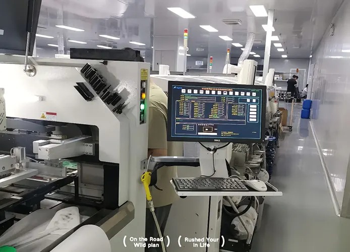
While SMT lines may appear identical on the surface, experienced manufacturers know that identical machines can produce drastically different results.
This discrepancy arises from the underlying process control, often overlooked by competitors who focus solely on automation speed.
SMT is fundamentally a controlled chemical and mechanical system, not just a matter of robotic placement.
Four pillars govern its success: process parameters, equipment capability, material consistency, and inspection strategy.
Minor variations in any pillar can lead to significant yield differences.
For example, solder paste viscosity changes with temperature and storage conditions.
A paste that is too thick may result in insufficient wetting, while a paste that is too thin can spread and create bridging.
Reflow temperature profiles must balance ramp, soak, and spike stages; even a ±5°C variation can lead to tombstoning of fine-pitch components.
Placement force must be precisely calibrated—too high and components deform, too low and misalignment occurs.
| Critical Variable | Typical Range / Tolerance | Failure Risk if Mismanaged |
|---|---|---|
| Solder paste viscosity | 80–120 Pa·s | Insufficient wetting, bridging |
| Reflow temperature (PCB top) | 220–250°C peak | Tombstoning, cold joints |
| Placement force | 0.1–0.5 N per 0402 | Component deformation, misalignment |
SMT Components and Packages: Design Impact on Assembly
The choice of component package has far-reaching effects on cost, yield, and inspection difficulty.
Consider the differences between QFN, BGA, and QFP:
- QFN and BGA packages provide excellent electrical performance and density but demand high-precision placement and X-ray inspection.
- Micro components such as 0201 and 01005 present placement challenges, increasing both setup time and defect probability.
- Bottom-termination components complicate inspection since solder joints are hidden from optical systems.
| Package Type | Assembly Complexity | Inspection Difficulty | Cost Implication |
|---|---|---|---|
| QFN | High | X-ray required | +10–20% over standard packages |
| BGA | Very High | X-ray mandatory | +20–30% due to rework risk |
| QFP | Moderate | AOI sufficient | +5–10% |
| 0201/01005 | Extremely High | Limited AOI | +25–40% setup cost |
Designers must weigh electrical performance versus manufacturability.
The most elegant circuit design can fail if it ignores the limitations of current SMT equipment and inspection capabilities.
Design for Manufacturability (DFM): The Stage That Decides Everything
The majority of SMT failures originate at the design stage. A perfectly tuned assembly line cannot compensate for poor PCB layout or inadequate pad design.
DFM principles guide designers to anticipate manufacturing constraints and minimize defects.
Pad symmetry is critical; asymmetric pads can cause tombstoning on passive components.
Spacing rules prevent solder bridging between adjacent pads or fine-pitch leads. Thermal balance must be maintained across the board to ensure uniform solder reflow.
Stencil design affects paste volume and distribution, while panelization strategy impacts throughput and rework efficiency.
| DFM Consideration | Design Recommendation | Impact on SMT Yield |
|---|---|---|
| Pad symmetry | Mirror pads across component axis | Reduces tombstoning |
| Spacing | ≥0.2 mm for 0603 components | Reduces bridging |
| Thermal balance | Equal copper distribution | Prevents cold joints |
| Stencil design | Aperture 1:1 ratio with pad | Ensures correct paste volume |
| Panelization | Optimize board orientation & fiducials | Improves placement accuracy, reduces rework |
Cost Drivers in SMT Assembly
SMT costs are not arbitrary; they are driven by component complexity, PCB design intricacy, number of reflow cycles, inspection requirements, and setup costs such as stencil fabrication and pick-and-place programming.
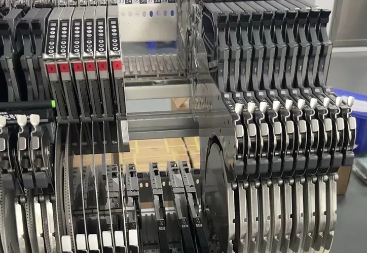
Fine-pitch BGAs and ultra-micro components substantially increase both assembly risk and cost.
Double-sided assemblies require additional reflow passes, further elevating production complexity.
Even the choice of panelization and board utilization can meaningfully affect the cost per unit.
| Cost Driver | Typical Impact on Quote |
|---|---|
| Component complexity (BGA, fine pitch) | +10–30% per board |
| PCB design complexity | +5–15% due to setup and risk |
| Number of reflow cycles | +5–10% per additional pass |
| Inspection requirements | +5–20% depending on X-ray / ICT |
| Setup costs | +$50–$200 per stencil/programming |
Cost optimization strategies include reducing unique components in the BOM, favoring standard packages like 0603 or 0805, minimizing double-sided assemblies where possible, and maximizing panel utilization.
Proper design planning in combination with strategic assembly choices can reduce SMT costs by 20–30% without sacrificing yield.
Common SMT Defects: Root Causes and Engineering Solutions
SMT defects are often predictable and preventable with careful design and process control.
Tombstoning typically arises from thermal imbalance and asymmetric pad design. Solder bridging occurs due to incorrect stencil apertures or paste inconsistencies.
Cold joints result from insufficient thermal energy during reflow, while misalignment often stems from placement errors or misread fiducials.
| Defect | Primary Cause | Engineering Solution |
|---|---|---|
| Tombstoning | Thermal imbalance, pad asymmetry | Adjust reflow profile, symmetric pads |
| Solder bridging | Paste over-volume, stencil error | Optimize stencil design, paste control |
| Cold joints | Insufficient reflow heat | Reflow profile tuning, thermal balancing |
| Misalignment | Placement error, fiducial misread | Calibrate machine, optimize fiducial layout |
Why SMT Enables High-Frequency and High-Speed Electronics
Surface-Mount Technology inherently supports high-frequency and high-speed electronic designs due to its physical and electrical characteristics.
The short interconnect lengths achievable with SMT reduce parasitic inductance and capacitance, which are critical factors in maintaining signal integrity at GHz frequencies.
Compared with Through-Hole Technology (THT), which often introduces longer leads and loops, SMT significantly lowers electromagnetic interference (EMI) and signal loss.
These advantages are particularly pronounced in RF circuits and high-speed digital systems.
For instance, GHz-level digital designs, such as DDR memory buses or high-speed serial interfaces, rely on controlled impedance and minimal interconnect parasitics.
THT components, with longer leads and inconsistent solder joints, struggle to maintain these characteristics.
| Parameter | SMT | THT | Impact on High-Speed Systems |
|---|---|---|---|
| Lead length | 0.2–0.5 mm | 1–5 mm | Shorter leads reduce parasitic inductance |
| Interconnect capacitance | 0.1–0.5 pF | 0.5–2 pF | Lower capacitance preserves signal integrity |
| EMI susceptibility | Low | Higher | Reduced loop area minimizes radiated emissions |
The combination of shorter interconnects and smaller package sizes enables SMT to handle the stringent electrical requirements of high-speed and RF applications, effectively making it the default choice for modern electronic systems.
Limitations of SMT: Where It Still Falls Short
Despite its many advantages, SMT is not without limitations.
Mechanical strength is inherently lower compared to THT due to the lack of through-hole anchoring, which can be critical in high-vibration environments such as automotive or aerospace applications.
Rework and repair are more challenging; micro-sized components, hidden solder joints under QFN or BGA packages, and dense layouts make manual repair difficult.
Thermal sensitivity is another constraint. Components with low thermal mass are prone to damage if reflow profiles are not carefully controlled, and hidden joints complicate inspection.
While advanced X-ray inspection can detect many hidden defects, it adds cost and may not catch every micro-void or crack.
| Limitation | Description | Mitigation Strategies |
|---|---|---|
| Mechanical strength | Susceptible to vibration and shock | Hybrid assembly, mechanical reinforcement |
| Repair difficulty | Hidden joints, micro-components | X-ray guided rework, preemptive DFM |
| Thermal sensitivity | Low-mass components overheat | Optimized reflow profiles, thermal balancing |
| Inspection challenges | Hidden solder joints | AOI + X-ray inspection, enhanced process monitoring |
Understanding these limitations is critical when designing systems that combine high-speed performance with mechanical robustness or when considering post-assembly maintenance.
Future Trends in SMT Technology
The evolution of SMT continues to be driven by miniaturization, integration, and automation.
Ultra-miniaturization pushes beyond 01005 components, demanding higher precision in printing, placement, and inspection.
Advanced packaging formats, such as System-in-Package (SiP) and Chip-Scale Packages (CSP), allow increased functionality in smaller footprints while reducing interconnect parasitics, further enabling high-frequency applications.
Artificial intelligence and machine learning are being integrated into inspection systems to detect defects beyond human or traditional AOI capability.
Smart factories aligned with Industry 4.0 principles leverage real-time process monitoring, predictive maintenance, and adaptive process control, ensuring consistent yield even in ultra-dense assemblies.
| Trend | Description | Potential Impact |
|---|---|---|
| Ultra-miniaturization | Components ≤01005 | Higher density, reduced parasitics |
| Advanced packaging (SiP, CSP) | Multi-die integration | Lower signal path, increased functionality |
| AI-driven inspection | Machine learning-based defect detection | Reduced rework, higher yield |
| Smart factories | Real-time process monitoring | Consistent quality, predictive optimization |
| Increased integration density | Denser PCB layouts | Smaller devices, higher performance |
Conclusion: SMT as the Core of Electronics Manufacturing
SMT is far more than a component assembly method. It is the central enabler of modern electronics, bridging design, manufacturing, and system-level performance.
The true value of SMT lies not just in automated placement and soldering but in its integration of good design, precise process control, and manufacturing expertise.
By understanding the interplay between component choice, DFM, process control, and inspection, manufacturers can unlock high yield, high-frequency performance, and cost-effective production.
SMT’s role as a system-level capability—rather than a simple process—ensures it will remain the backbone of electronics manufacturing in both current and next-generation technologies.
References
- IPC-7351B: Generic Requirements for Surface Mount Design and Land Pattern Standard, IPC, 2020
- ASM International, SMT Handbook, 2021
- J. K. Lindahl, SMT Process Control, SMTA International, 2020
- Pozar, Microwave Engineering, 5th Edition, Wiley, 2021
- IEEE Transactions on Components, Packaging and Manufacturing Technology, 2022