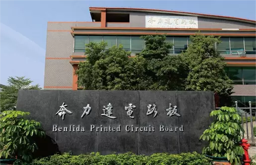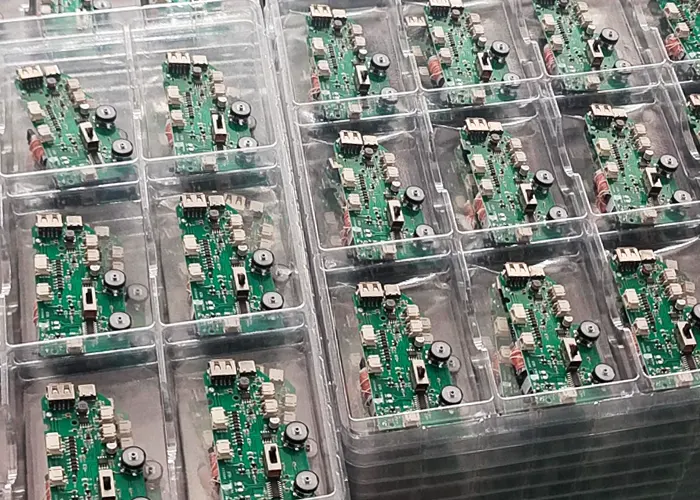
In modern electronics manufacturing, Printed Circuit Board Assembly (PCBA) is often simplified as “placing components on a board.” This description is technically incomplete. In reality, PCBA is a tightly coupled, multi-physics process involving materials science, thermal dynamics, mechanical precision, and supply chain coordination.
A typical SMT production line operates at placement speeds exceeding 100,000 components per hour (CPH), with positional accuracy within ±25–50 μm. At this scale, even minor deviations in solder paste rheology or component coplanarity can propagate into systemic defects.
The hidden complexity lies in process interdependence. For example, a minor design imbalance in copper distribution can induce uneven thermal gradients during reflow, leading to tombstoning or warpage. Similarly, supply chain substitutions can alter wetting characteristics due to differences in metallization finishes.
This 2026 guide examines the full PCBA workflow, focusing not only on process steps but also on risk concentration points and optimization strategies grounded in manufacturing data and engineering principles.
The Complete PCB Assembly Flow at a Glance
The PCBA process can be abstracted into a closed-loop manufacturing system:
Design → DFM Validation → Material Preparation → Printing → Placement → Reflow → Inspection → Testing → Delivery
Each stage introduces distinct constraints on time (T), cost (C), and yield (Y). These variables are often modeled using a simplified manufacturing efficiency relationship:
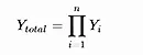
Where:
- Yi = yield of each process step
- Ytotal = cumulative production yield
Even a high-performing line with 98% yield per step across 8 steps results in:

This illustrates why early-stage optimization is critical.
SMT vs THT: Process Characteristics
| Parameter | SMT (Surface Mount Technology) | THT (Through-Hole Technology) |
|---|---|---|
| Assembly Speed | Very high (automated) | Low to medium |
| Mechanical Strength | Moderate | High |
| Component Density | Very high | Limited |
| Cost Efficiency | High for volume production | Higher labor cost |
| Typical Use Cases | Consumer electronics | Power, aerospace, automotive |
In current industry practice, over 85–90% of components in commercial electronics are assembled via SMT, with THT reserved for high-reliability or high-load applications (IPC, 2024).
Step 0: Design & DFM — The Stage That Decides Everything
Design for Manufacturability (DFM) is statistically the most influential stage in PCBA. Industry analyses indicate that over 70% of manufacturing defects originate from design-stage decisions (Siemens EDA, 2023).
At this stage, engineers must reconcile electrical performance with manufacturing constraints.
Critical Design Parameters
| Parameter | Engineering Constraint | Impact on Assembly |
|---|---|---|
| Pad spacing | ≥ IPC-7351 standards | Prevents solder bridging |
| Footprint match | Component-specific | Ensures alignment accuracy |
| Thermal balance | Symmetrical copper | Prevents tombstoning |
| Via-in-pad | Requires filling | Avoids solder loss |
Thermal imbalance can be quantified using a simplified heat distribution model:
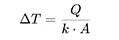
Where:
- ΔT = temperature gradient
- Q = heat input
- k = thermal conductivity
- A = copper area
Uneven copper distribution increases ΔT, leading to differential wetting forces during reflow.
A common failure scenario arises when a design passes simulation but fails during mass production. Simulation environments often assume ideal material uniformity, whereas real production includes variability in solder paste deposition, component tolerances, and oven profiles.
Step 1: BOM & Supply Chain — The Hidden Bottleneck
While often overlooked, the Bill of Materials (BOM) stage is a primary determinant of production continuity and quality stability.
Supply Chain Realities in 2026
The electronics industry continues to face:
- Cyclical semiconductor shortages
- Extended lead times (up to 40–60 weeks for certain ICs)
- Increased reliance on cross-qualified substitutes
Two sourcing models dominate:
| Model | Description | Advantages | Risks |
|---|---|---|---|
| Turnkey | Supplier handles full procurement | Simplified logistics | Less control over sourcing |
| Consigned | Customer supplies components | Full control | High coordination complexity |
A critical risk in this stage is counterfeit or obsolete components, particularly in broker-sourced supply chains. According to ERAI (2024), counterfeit incidents increased by ~15% year-over-year in constrained markets.
Material authenticity directly affects solderability. For instance, oxidation on component leads reduces wetting force:

Where:
- γ = surface tension
- θ = angle (contact angle)
Higher oxidation increases θ, reducing wetting efficiency and increasing defect probability.
Step 2: Solder Paste Printing — Small Layer, Big Impact
Solder paste printing is widely recognized as the single most critical step in SMT, contributing to approximately 50–70% of all assembly defects (ASM Assembly Systems, 2023).
The process involves depositing a controlled volume of solder paste onto PCB pads using a stencil. The quality of this thin layer—typically 100–150 μm thick—directly determines joint reliability.
Process Control Parameters
| Parameter | Typical Range | Effect |
|---|---|---|
| Stencil thickness | 80–150 μm | Controls paste volume |
| Aperture design | Area ratio > 0.66 | Ensures proper release |
| speed | 20–80 mm/s | Affects uniformity |
| Squeegee pressure | 0.5–1.0 N/mm | Impacts fill consistency |
A critical design metric is the Area Ratio (AR):
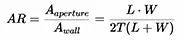
Where:
- L,W = aperture length and width
- T = stencil thickness
If AR<0.66, paste release becomes unreliable, leading to insufficient deposits.
Failure Modes and Mechanisms
- Excess paste (bridging): Caused by oversized apertures or low-viscosity paste
- Insufficient paste: Due to poor stencil release or contamination
- Slumping: low paste viscosity or high ambient temperature
Even minor volumetric deviations (±10–15%) can significantly impact joint geometry and reliability, especially for fine-pitch components (<0.5 mm).
Step 3: Pick-and-Place — Where Speed Meets Precision
In modern surface-mount assembly, the pick-and-place stage defines both throughput and placement accuracy. High-speed placement machines routinely achieve rates between 30,000 and 100,000 components per hour (CPH), depending on machine architecture (turret vs. gantry) and component mix. The underlying principle combines machine vision, motion control, and vacuum-based pickup systems to ensure accurate component alignment before placement.
A simplified positioning model illustrates the relationship between placement accuracy and mechanical tolerances:

Where:
- Evision: camera recognition error
- Emechanical: gantry movement deviation
- Eboard: PCB warpage or fiducial misalignment
As component sizes shrink to 01005 packages (0.4 mm × 0.2 mm), tolerances tighten dramatically. Placement accuracy must typically remain within ±25 µm or better. At this scale, even slight deviations in nozzle wear, feeder calibration, or PCB flatness can result in misalignment.
The risk is not merely cosmetic. A micron-level offset can lead to insufficient solder wetting, bridging, or open circuits after reflow. Consequently, manufacturers increasingly rely on closed-loop feedback systems, where real-time inspection data is used to recalibrate placement parameters dynamically.
Step 4: Reflow Soldering — The Most Critical Thermal Process
Reflow soldering transforms deposited solder paste into reliable electrical and mechanical joints through a carefully controlled thermal profile. The process typically consists of four stages: preheat, soak, reflow, and cooling.
The thermal behavior can be approximated by heat transfer principles:
Q = mcΔT
Where:
- Q: heat energy absorbed
- m: mass of the assembly
- c: specific heat capacity
- ΔT: temperature change
A standard lead-free reflow profile peaks at 235–250°C, with a time above liquidus (TAL) of 30–90 seconds. Maintaining this balance is critical. Overheating can degrade components or cause excessive intermetallic growth, while insufficient heat leads to incomplete solder wetting.
Two common defects illustrate this sensitivity:
- Tombstoning occurs when uneven wetting forces lift one end of a small component. This is often caused by temperature gradients or asymmetric pad design.
- Cold joints result from inadequate melting, leading to weak mechanical bonds and high electrical resistance.
The relationship between wetting force imbalance and defect formation can be qualitatively expressed as:
Fnet=Fleft−Fright
A non-zero net force increases the likelihood of component displacement during reflow.
In practice, precise oven zoning, conveyor speed control, and solder paste formulation are all tuned to minimize these risks.
Step 5: Through-Hole & Mixed Assembly — Strength vs Efficiency
Despite the dominance of surface-mount technology, through-hole technology (THT) remains essential in applications requiring mechanical robustness, such as connectors, transformers, and high-power components. The mechanical strength of a through-hole joint is significantly higher due to the plated hole anchoring effect.
Mixed assembly introduces both SMT and THT components on the same board, requiring careful process planning. Two primary soldering methods are used:
| Parameter | Wave Soldering | Selective Soldering |
|---|---|---|
| Process Type | Full-board immersion | Targeted solder application |
| Throughput | High | Moderate |
| Flexibility | Low | High |
| Thermal Stress | Higher | Lower |
| Typical Use Case | High-volume THT boards | Mixed or complex assemblies |
A common design mistake is failing to consider process compatibility when mixing SMT and THT. For example, placing sensitive SMT components on the underside of a board intended for wave soldering can expose them to excessive thermal stress or solder contamination.
Effective design for mixed assembly requires synchronized layout planning, including component orientation, keep-out zones, and thermal shielding strategies.
Step 6: Inspection — Catching Invisible Problems
Inspection in PCB assembly is not a single step but a multi-stage quality control strategy. The goal is to detect defects as early as possible, where correction costs are significantly lower.
Two dominant inspection technologies are widely used:
| Inspection Method | Detection Capability | Limitation |
|---|---|---|
| AOI (Automated Optical Inspection) | Component presence, polarity, solder bridges, misalignment | Cannot see hidden joints (e.g., BGAs) |
| X-ray Inspection | Hidden solder joints, voids, BGA integrity | Higher cost, slower throughput |
AOI systems rely on image comparison algorithms and can inspect thousands of components per minute. X-ray systems, on the other hand, use density contrast to analyze internal solder structures, making them indispensable for advanced packages like BGAs and QFNs.
The economic impact of early defect detection can be modeled as:

Where n represents the production stage (e.g., soldering, assembly, field). A defect caught during solder paste inspection may cost cents to fix, while the same defect discovered in the field could cost hundreds of dollars due to returns, repairs, and reputational damage.
Step 7: Testing — Does the Board Actually Work?
Inspection ensures the board is built correctly; testing ensures it functions correctly. These are fundamentally different objectives.
Two primary testing methods are used in PCB assembly:
| Test Method | Purpose | Coverage Level |
|---|---|---|
| In-Circuit Testing (ICT) | Verifies individual components and connections | High structural coverage |
| Functional Testing (FCT) | Validates real-world operation | High functional coverage |
ICT uses a bed-of-nails fixture to probe test points on the PCB, measuring parameters such as resistance, capacitance, and continuity. Functional testing, by contrast, powers the board and evaluates its performance under simulated operating conditions.
An important aspect of modern testing is firmware programming. Many boards require microcontrollers or programmable devices to be flashed before functional validation. Errors at this stage—such as incorrect firmware versions or programming failures—can render an otherwise perfect assembly non-functional.
This highlights a critical reality in electronics manufacturing: visual perfection does not guarantee electrical integrity. Latent defects such as marginal solder joints, incorrect component values, or firmware mismatches may only surface during functional testing.
Step 8: Rework & Repair — The Cost Nobody Talks About
Even in highly optimized SMT lines, rework is unavoidable. Industry data indicates that first-pass yield (FPY) for complex assemblies typically ranges from 92% to 98%, meaning a small but significant percentage of boards require correction before shipment. While this may appear minor, the cumulative impact on cost and lead time is substantial.
The cost escalation associated with rework can be modeled using a simplified relationship:
Ctotal=Cbase+n⋅Crework+Cdelay
Where:
- Cbase: original manufacturing cost
- n: number of rework iterations
- Crework: cost per repair cycle
- Cdelay: cost associated with production delays
Rework operations—such as component removal, pad cleaning, and re-soldering—introduce thermal stress that can degrade PCB laminate integrity or damage sensitive components. For example, repeated exposure to reflow temperatures can increase the risk of pad lifting or delamination, especially in high-density or thin-core boards.
From a production perspective, rework disrupts line flow and reduces throughput. A board that undergoes even a single rework cycle may experience lead time extensions of 10–30%, depending on complexity and inspection requirements.
The most effective strategy to minimize rework is not better repair capability, but better design. Design for Manufacturability (DFM) principles—such as proper pad geometry, balanced copper distribution, and adequate spacing—can significantly reduce defect rates before they occur.
Step 9: Cleaning, Coating & Final Assembly
After soldering and rework, the PCB assembly enters a stage that is often underestimated but critical for long-term reliability: cleaning and protection.
Flux residues left on the board can be ionic or non-ionic contaminants, which may lead to corrosion, dendritic growth, or electrical leakage under humid conditions. The effectiveness of cleaning is often quantified by ionic contamination levels:
Ionic Contamination ≤ 1.56 μg/cm2 (NaCl equivalent)
This threshold, commonly referenced in industry standards, ensures that residues do not compromise electrical performance over time.
Cleaning methods vary from aqueous washing to solvent-based and semi-aqueous processes, depending on flux type and board complexity. No-clean fluxes reduce cleaning requirements but do not eliminate the need entirely in high-reliability applications.
Conformal coating adds an additional protective layer, particularly for assemblies operating in harsh environments such as automotive, aerospace, or industrial control systems. Coating materials—including acrylics, silicones, and urethanes—provide resistance against moisture, dust, and chemical exposure.
| Coating Type | Key Property | Typical Application |
|---|---|---|
| Acrylic | հեշտ rework, fast drying | Consumer electronics |
| Silicone | High temperature stability | Automotive, power electronics |
| Urethane | chemical resistance | Industrial environments |
Final assembly, often referred to as box-build integration, involves installing the PCB into its enclosure, connecting wiring harnesses, and integrating mechanical components. At this stage, system-level considerations such as thermal management, vibration resistance, and electromagnetic compatibility become critical.
Step 10: Packaging & Delivery — Protecting the Final Product
Once the assembly is complete and tested, attention shifts to ensuring that the product reaches the customer without degradation. Electrostatic discharge (ESD) and mechanical shock are the two primary risks during handling and shipping.
ESD sensitivity is measured in terms of voltage thresholds, with many modern ICs vulnerable at levels below 100 V. Proper packaging materials—such as anti-static bags, conductive foam, and shielding containers—are designed to dissipate or block electrostatic charges.
The probability of shipping damage can be conceptually linked to handling stress:

Where:
- Sshock: impact forces during transit
- Svibration: continuous mechanical stress
- Shandling: human-induced risks
Protective packaging solutions, including custom foam inserts and rigid cartons, are engineered to absorb these stresses. International shipping standards, such as ISTA testing protocols, are often used to validate packaging effectiveness.
Beyond physical protection, labeling and traceability are equally important. Barcodes, serial numbers, and batch tracking ensure that products can be identified and recalled if necessary.
Quality Standards That Define Reliability
Quality in PCB assembly is governed by internationally recognized standards that define acceptance criteria and manufacturing practices. Among the most widely adopted are the standards developed by IPC.
The IPC classification system categorizes electronic products into three classes:
| Class | Description | Typical Applications |
|---|---|---|
| Class 1 | General electronics, limited lifespan | Consumer devices |
| Class 2 | Dedicated service electronics, higher reliability | Industrial equipment |
| Class 3 | High-reliability, mission-critical systems | Aerospace, medical, defense |
Class 3 assemblies require the strictest criteria, including tighter tolerances, enhanced inspection, and higher workmanship standards.
In addition to IPC, quality management systems such as ISO standards play a crucial role. International Organization for Standardization provides frameworks like ISO 9001, which ensures consistent process control and continuous improvement.
Environmental compliance is addressed through regulations such as Restriction of Hazardous Substances Directive, which restricts the use of hazardous materials like lead, mercury, and cadmium in electronic products.
Choosing the appropriate quality level depends on the application. While Class 3 offers maximum reliability, it also increases cost due to stricter inspection and process controls. For many commercial products, Class 2 provides a balanced approach between performance and cost efficiency.
Most Common PCB Assembly Problems (and How to Avoid Them)
Despite advances in automation and process control, certain defects continue to appear across PCB assembly lines. Understanding their root causes is essential for prevention.
| Defect Type | Description | Primary Root Cause |
|---|---|---|
| Solder Bridging | Unintended connection between pads | Excess solder, poor stencil design |
| Tombstoning | Component lifts on one end | অসম balanced wetting forces |
| Misalignment | Component shifted from pad center | Placement error, PCB warpage |
These defects rarely originate from a single source. Instead, they typically result from interactions between design, materials, and process parameters.
For instance, solder bridging may be caused by excessive paste deposition (process), but the underlying issue could be insufficient pad spacing (design). Similarly, tombstoning is often linked to uneven thermal profiles (process), but pad geometry and copper balancing (design) also play a critical role.
A useful way to conceptualize defect formation is through a multi-factor model:
D=f(Ddesign,Dprocess,Dmaterials)
Where:
- Ddesign: layout, pad geometry, spacing
- Dprocess: printing, placement, reflow conditions
- Dmaterials: solder paste, PCB substrate, components
Reducing defect rates, therefore, requires a holistic approach. Collaboration between design engineers, process engineers, and material suppliers is essential to identify and eliminate root causes early in the product lifecycle.
SMT vs THT: Which Should You Choose in 2026?
The choice between surface-mount technology (SMT) and through-hole technology (THT) is no longer a binary decision in 2026. Instead, it is a strategic trade-off between density, automation, mechanical strength, and cost efficiency.
SMT dominates modern electronics because it enables high-density designs and automated assembly. In high-volume production, automated placement significantly reduces labor cost per component. By contrast, THT remains relevant for components that require strong mechanical anchoring, such as connectors, transformers, and high-power devices. However, THT assembly is typically more labor-intensive, often adding $0.50 to $3.00 per component in manual insertion and soldering costs.
A practical decision framework can be summarized through engineering priorities:
| Decision Factor | SMT Advantage | THT Advantage |
|---|---|---|
| Component Density | High (supports miniaturization) | Low |
| Automation | Fully automated | Semi/manual |
| Mechanical Strength | Moderate | High |
| Cost (High Volume) | Lower | Higher |
| Repairability | Difficult | Easier |
with THT for structural or high-current elements. This mixed approach typically increases assembly cost by 10–15%, but significantly improves product robustness and design flexibility.
Cost Breakdown: Where Your Money Actually Goes
Understanding PCB assembly cost structure is essential for both budgeting and optimization. Contrary to common assumptions, labor is not always the dominant cost—materials and design decisions typically drive the majority of expenses.
Industry data shows that components alone account for 30–60% of total PCB assembly cost, making the Bill of Materials (BOM) the single largest contributor.
A representative cost distribution is shown below:
| Cost Category | Typical Share (%) | Key Drivers |
|---|---|---|
| Materials (PCB + BOM) | 30–60% | Component type, availability, PCB complexity |
| Assembly Process | 20–35% | Component count, placement complexity |
| Labor & Engineering | 10–20% | Skill level, automation level |
| Testing & Inspection | 5–15% | ICT, functional test, X-ray |
| NRE / Setup | 5–10% | Stencil, programming, tooling |
Cost sensitivity can be modeled as:
Ctotal=Cmaterials+Cprocess+Clabor+Ctesting+CNRE
Among these, component sourcing and design complexity have the highest impact. For example, using fine-pitch BGAs or ultra-small components can increase assembly cost by 20–100% due to tighter tolerances and inspection requirements.
Equally important is production volume. Due to fixed setup costs, low-volume prototypes can cost $30–$80 per board, while high-volume production may drop below $5 per board.
Cost reduction, therefore, is less about negotiation and more about engineering decisions. Simplifying PCB layers, using standard component packages, and avoiding unnecessary complexity can reduce costs without sacrificing quality.
Future Trends in PCB Assembly (2026 and Beyond)
PCB assembly is undergoing a transformation driven by automation, data integration, and sustainability requirements.
Artificial intelligence is increasingly embedded in inspection systems. AI-powered AOI can now detect subtle defects—such as marginal solder joints or early-stage delamination—that traditional rule-based systems may miss. This improves detection rates while reducing false positives, leading to more stable production yields.
At the factory level, the concept of the “smart factory” is becoming mainstream. Equipment is interconnected through Industrial IoT (IIoT), enabling real-time monitoring of machine performance, predictive maintenance, and adaptive process control. This directly improves equipment utilization, which can increase from 65–75% to over 85–95% with optimized systems.
Miniaturization continues to push the limits of manufacturing. With widespread adoption of 01005 and even smaller packages, placement accuracy, inspection resolution, and thermal control must evolve simultaneously.
Sustainability is also becoming a key driver. Lead-free soldering (aligned with Restriction of Hazardous Substances Directive compliance) and energy-efficient manufacturing processes are no longer optional but expected in global supply chains.
Practical Checklist Before Sending Your PCB for Assembly
Before releasing a design to manufacturing, preparation determines success. Incomplete or inconsistent documentation remains one of the most common causes of delays and defects.
A structured readiness checklist ensures alignment between design and production:
| Category | Key Requirements | Risk if Missing |
|---|---|---|
| Design Files | Gerber, drill, pick-and-place, stencil data | Misalignment, incorrect fabrication |
| BOM | Complete part numbers, quantities, alternatives | Component shortages, cost overruns |
| Assembly Drawing | Polarity, orientation, special instructions | Placement errors |
| Testing Plan | ICT points, functional test procedures | Undetected electrical failures |
| Compliance | RoHS, material declarations, certifications | Regulatory rejection |
Beyond documentation, communication with the manufacturer is critical. Clarifying requirements such as acceptable substitutions, inspection criteria, and test coverage can prevent costly misunderstandings later in production.
Conclusion: How to Ensure a Successful PCB Assembly Project
PCB assembly is not a single process but an integrated system where design, materials, manufacturing, and quality control interact continuously. Failures rarely originate from one step; they emerge from misalignment across multiple stages.
Several key insights define successful projects:
- Design decisions determine cost and yield more than manufacturing itself
- Early defect prevention is exponentially cheaper than late-stage correction
- Testing validates function, not just appearance
The integration of design and process is therefore essential. Engineers must consider manufacturability, inspection, and testing from the earliest design phase, rather than treating them as downstream concerns.
Equally important is choosing the right manufacturing partner—one that offers not only technical capability but also transparency, process control, and engineering support. In an era of increasing complexity and shrinking tolerances, collaboration between design teams and manufacturers is the most reliable path to consistent, high-quality outcomes.