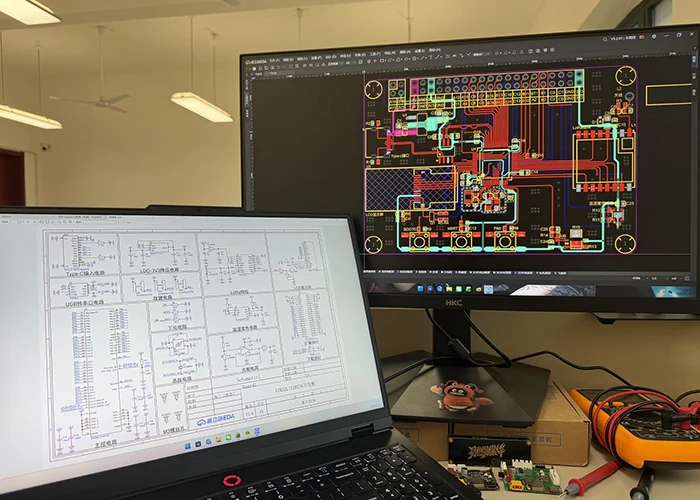
The layout of components on a PCB is of critical importance. A correct and reasonable layout not only makes the board look neater and more aesthetically pleasing, but also affects the length and number of printed conductors.
A well-designed PCB component layout is of paramount importance for enhancing the overall performance of the device.

6 Key Details for Improving PCB Layout Quality
Key Layout Considerations for Wireless Modules
Designers should avoid placing high-frequency digital traces, high-frequency analog traces, power traces, and other sensitive components directly beneath the wireless module, although copper can be laid beneath the module.
The layout should position the wireless module as far as possible from components that generate significant electromagnetic interference, such as transformers, high-power inductors, and power supplies.
When using modules with on-board PCB antennas or ceramic antennas, the design must leave the PCB area directly beneath the antenna section free of copper. The antenna section should also be placed as close as possible to the board edge.
The layout should minimize the length of both RF signal traces and other signal traces.
The design should also keep other signals away from the wireless module’s transmitting section to avoid interference.
The layout must ensure a complete power ground path for the wireless module, and RF traces should include sufficient space for grounding vias.
The wireless module has strict requirements for voltage ripple;
Therefore, it is best to add an appropriate filtering capacitor, such as a 10uF capacitor, near the module’s voltage pins;
Wireless modules operate at high transmission frequencies, which impose certain requirements on the power supply’s transient response.
Designers should select a high-performance power supply solution during the design phase.
The layout should also arrange the power circuit in a reasonable manner to fully utilize the performance of the power supply.
For example, in DC-DC converter layouts, the ground connection of the freewheeling diode should be placed as close as possible to the IC ground to ensure proper current return, and the power inductor and capacitor should be positioned as close as possible to each other.
Setting Trace Width and Spacing
The configuration of trace width and spacing has a significant impact on the overall performance of the board.
Properly setting trace width and spacing can effectively improve the board’s electromagnetic compatibility (EMC) and overall performance.
Power trace width design requires consideration of multiple factors.
These factors include the device’s load current, supply voltage, PCB copper thickness, and trace length.
Typically, a 1.0 mm wide trace with 1 oz copper thickness can handle a current of approximately 2 A.
Properly setting trace spacing can effectively reduce phenomena such as crosstalk.
For instance, the commonly used 3W rule (i.e., when the center-to-center spacing between traces is no less than three times the trace width, 70% of the electric fields will not interfere with each other) is a useful guideline.
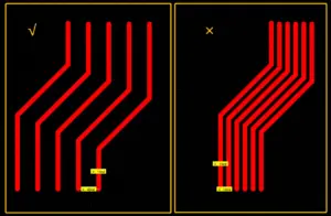
Power Trace Design Guidelines
Power Tracing: A comprehensive assessment of the load’s current, voltage, and PCB copper thickness determines the required current capacity.
The design should typically set the current capacity to at least twice the normal operating current.
The layout should also follow the 3W rule for trace spacing as closely as possible.
Signal and RF Trace Design Considerations
Signal Tracing: Based on a comprehensive assessment of the signal’s transmission speed, type (analog or digital), and trace length, the recommended spacing for standard signal traces is to follow the 3W rule; differential traces require separate consideration.
RF Tracing: The trace width for RF traces must account for characteristic impedance.
Common RF module antenna interfaces typically have a characteristic impedance of 50Ω.
As a rule of thumb, the design should use a trace width of 0.55 mm and a copper spacing of 0.5 mm for RF traces with power ≤30 dBm (1 W).
For greater accuracy, the board manufacturer can assist in adjusting the design to achieve a characteristic impedance of approximately 50Ω.
Component Spacing Requirements
Component Spacing: When designing the PCB layout, component spacing is a critical consideration.
If spacing is too small, it can lead to solder bridging, which may affect production.
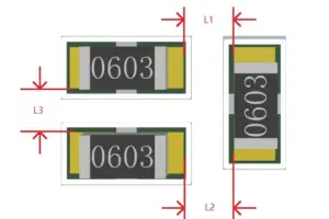
The recommended spacing is as follows:
Same component type: ≥0.3 mm;
Different component types: ≥0.13*h + 0.3 mm (where h is the maximum height difference among adjacent components);
The layout should maintain a minimum spacing of 1.5 mm between components that require manual soldering.
The layout should also maintain 1–3 mm spacing between through-hole and surface-mount components.
PCB Edge Clearance and Mechanical Safety
Controlling the Clearance Between Board Edges and Components/Traces:
When laying out and routing a PCB, the design must maintain appropriate spacing between components, traces, and the board edges.
In actual production, manufacturers commonly use panelization processes.
If the layout positions components too close to the board edge, PCB separation can detach pads or even damage the components.
Similarly, if traces are too close to the edge, they are prone to breaking during production, which can impair circuit functionality.
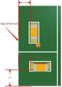
Recommended Placement and Edge Clearance Standards
Recommended Spacing and Placement:
Component Placement: The layout design should align component pads parallel to the “V-cut” direction of the panel.
This ensures that the mechanical stress on the component pads during panel separation is uniform and directed in the same direction, thereby reducing the likelihood of pad detachment.
Component Spacing: The layout design should ensure that components are placed at least 0.5 mm away from the board edge.
Trace Spacing: The layout design should also ensure that traces are placed at least 0.5 mm away from the board edge.
Connecting Adjacent Pads and Teardrop Shapes
The design should avoid directly connecting adjacent IC pins on the pads when such connections are required.
Instead, route the connection outside the pads to prevent solder bridges between the IC pins during production.
The design should also control the width of traces routed between adjacent pads.
Ideally, these traces should not exceed the width of the IC pins, except in special cases such as power pins.

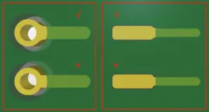
Teardrops effectively reduce reflections caused by sudden changes in trace width, ensuring a smooth connection between the trace and the pad;
Adding teardrops resolves the issue of the connection between the trace and the pad breaking easily when subjected to impact.
Via Parameters and Placement
The appropriate sizing of vias has a significant impact on circuit performance.
Optimal via size selection depends on factors such as via current-carrying capability, signal frequency, and manufacturing complexity.
The PCB layout process must carefully account for these factors to ensure proper design performance.
When space is extremely limited, the design may place vias directly on pads.
The board manufacturer can support this through-hole manufacturing process. However, this approach increases production costs.
Key Points for Via Design:
A single PCB may include vias of different sizes to meet varying trace requirements.
However, the design should limit the number of via types to no more than three to prevent significant production complexity and increased manufacturing costs.
The depth-to-diameter ratio of vias should generally be ≤6, as ratios exceeding 6 make it difficult to ensure uniform copper plating on the via walls during production;
Design considerations must include parasitic inductance and capacitance of vias, particularly in high-speed circuits where distributed parameters require special attention.
Smaller vias result in lower distributed parameters and are more suitable for high-speed circuits, but they also come with higher costs.
The 5 Most Common Design Mistakes in PCB Layout
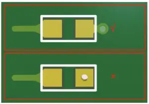
Pin Misalignment
Discrepancies between the design and the routing are the primary cause of errors in the final stages of PCB design.
Therefore, it is necessary to double-check certain aspects, such as component dimensions, via quality, pad sizes, and review levels.
In short, the design process requires repeated verification against the schematic.
Acid Traps
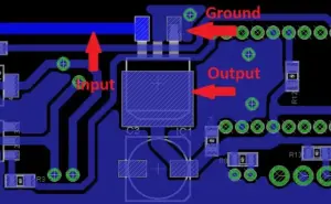
When the angle between PCB traces is too small (forming an acute angle), acid traps may form.
During the etching stage, etching solution may accumulate in these acute-angled connections, causing excessive removal of the copper layer in those areas and creating constrictions or traps.
This can eventually lead to trace fractures and open circuits.
Modern manufacturing processes that adopt photoresist etching solutions have significantly reduced the occurrence of acid traps.
Tombstoning
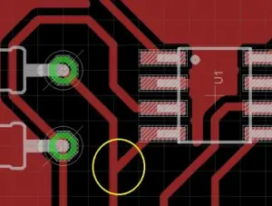
When soldering small surface-mount devices using a reflow process, the devices may experience one-sided warping due to solder wetting, a phenomenon commonly known as “tombstoning.”
Asymmetrical layout patterns typically cause this phenomenon by creating uneven heat distribution across the device pads.
Implementing proper DFM checks can effectively mitigate tombstoning.

Trace Width
When the current in a PCB trace exceeds 500 mA, the design should ensure appropriate trace width is selected.
Generally, traces on the surface of a PCB carry more current than those inside a multilayer board because surface traces can dissipate heat through airflow.
Trace width is also related to the copper foil thickness of the layer in question. Most PCB manufacturers allow you to choose copper foil thicknesses ranging from 0.5 oz/sq. ft to 2.5 oz/sq. ft.
PCB Layout Design for RJ45 Port Circuits
When designing an RJ45 module circuit PCB layout, the design process should follow the following key considerations.
1. The layout should position the network transformer component as close as possible to the RJ45 connector to minimize common-mode interference coupling.
2. When using a separate external PHY chip, place the PHY chip as close as possible to the downstream SOC processing chip to shorten the trace length between the PHY chip and the downstream SOC processing chip, thereby reducing radiated interference.
3. Position the DC-DC conversion chip and the power amplifier chip as far away as possible from the RJ45 connector and the network transformer components.
This layout reduces the risk that common-mode interference generated by the power circuitry will couple into the RJ45 differential signal current loop through Bob Smith common-mode coupling capacitors.
Such interference coupling can lead to failures in telecommunications conduction testing of the RJ45 interface.
4. The design should place the PHY chip and any external crystal oscillators used with it away from the board edges and connectors.

Conclusion
A well-executed PCB layout design is a fundamental factor in determining the electrical performance, reliability, and manufacturability of modern electronic systems.
Throughout the design process, careful attention must be given to wireless module placement, RF and high-speed signal routing, power integrity, component spacing, and edge clearance to minimize electromagnetic interference and ensure stable circuit operation.
Key layout practices—such as maintaining proper trace width and spacing (including the 3W rule), optimizing RF impedance control, ensuring proper via selection, and applying effective thermal and mechanical design considerations—collectively contribute to improved signal integrity and reduced production risks.
In addition, avoiding common design errors such as pin misalignment, acid traps, and tombstoning further enhances manufacturing yield and product robustness.
For interface-critical circuits such as RJ45 systems, strict component placement strategies are essential to suppress common-mode noise and maintain compliance with transmission standards.
Overall, disciplined adherence to PCB layout principles ensures not only functional correctness but also long-term stability, high performance, and efficient production scalability in electronic product design.