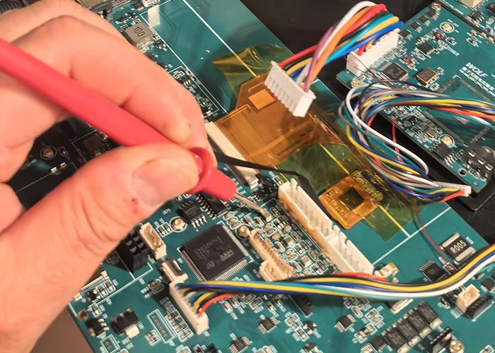
Advances in information technology have placed higher demands on electronic components in terms of miniaturization, high integration, high frequency, and low loss.
Introduction
As a key material for electronic packaging, low-temperature co-fired ceramics (LTCC) enable three-dimensional modular integration of electronic components.
With advantages such as compact size and high integration, LTCC has been widely adopted in fields such as aerospace, aviation, communications, and radar.
Challenges of Solder Wetting in LTCC Assembly
The assembly quality of surface-mount components on LTCC has always been a major focus within the industry, with the issue of solder wetting on non-soldered areas being particularly prominent.
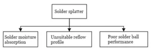
Solder wetting is primarily caused by solder splatter. Previous studies have extensively investigated the causes of solder splatter after reflow, focusing mainly on solder moisture absorption, reflow profiles, and solder properties.
Research findings indicate that solder moisture absorption is one of the primary causes of spatter, while the appropriateness of the reflow profile directly affects solder wettability and the risk of spatter.
Since conventional spatter on standard printed circuit boards does not cause significant issues and can generally be cleaned off, previous studies have not provided solutions.
However, LTCC is extremely sensitive to splatter; once splatter lands on the bonding area, the solder melts and spreads immediately, resulting in rework at best and scrap at worst.
Additionally, the composition and performance of the flux in the solder also have a significant impact on the splatter phenomenon.
Research Focus and Improvement Measures
Although previous studies have systematically investigated solder splatter issues, existing solutions remain inadequate for the specific requirements of LTCC.
Building upon previous research, this paper systematically analyzes the mechanism of solder wetting on LTCC after reflow soldering from three aspects: solder moisture absorption, reflow profiles, and solder performance, and proposes a comprehensive set of improvement measures.
The team implemented measures such as optimizing production processes and strictly controlling workshop temperature and humidity.
These actions significantly reduced the proportion of solder wetting on the gold layer in non-soldering areas and provided an important reference for the engineering application of LTCC technology.
Analysis of Solder Contamination
Solder contamination on the gold layer outside the soldering area is a major factor affecting the assembly quality of LTCC surface-mount components.
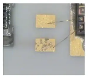
If the contamination occurs within the bonding area, it may affect the position of the bond points (Figure 1), leading to unstable circuit performance.
Operators can repair the gold layer after solder contamination by either scraping off the solder or applying a copper patch.
However, controlling this process is difficult, and it can easily scratch or damage the printed circuit lines (Figure 2).
Such scratches or damage may cause the production team to scrap the board.

Main Causes of Solder Contamination
Generally, there are three main causes of solder contamination on pads:
First, contamination during the printing process, where insufficient cleaning of the stencil leaves solder residue near the apertures on the B-side of the stencil, which then contaminates non-soldering areas during subsequent printing;
Second, operational errors during the soldering process, such as improper handling of LTCC boards or dirty rubber gloves, can cause solder to adhere to non-soldering areas;
Third, solder splatter during the reflow process—in the reflow oven, solder may splatter due to moisture absorption, an inappropriate reflow profile, or poor solder performance, resulting in solder adhering to the gold layer in non-soldering areas.
Challenges of Reflow Solder Splatter
As production automation continues to advance, the first two causes have been effectively controlled and resolved;
However, the issue of solder splatter during the reflow process remains difficult to completely avoid, posing a major challenge for the assembly of surface-mount components on LTCC boards.
Analysis of the Causes of Solder Splatter
Typically, the LTCC assembly process consists of six steps (Figure 3).

1) Solder paste printing on the B-side: The primary purpose is to reduce the void rate during the bonding of the LTCC substrate to the housing.
2) Flip: After applying solder paste to the B-side, operators flip the substrate so that the component mounting side faces upward
This reduces the number of reflow cycles, protects the substrate plating, and improves efficiency.
3) T-side solder paste printing: Operators apply solder paste to the pads where components are to be mounted using a stencil printing process.
4) Placement: The placement machine positions components in their respective locations.
5) Reflow: Operators perform soldering using a hot-air reflow oven.
They conduct the reflow process under a nitrogen atmosphere, controlling oxygen content below 0.2%.
6) Automated Optical Inspection (AOI): The AOI equipment inspects and records the quality of solder joints and solder coverage.
Process Analysis of Solder Contamination
Through this process, the current rate of solder contamination on non-soldering area gold layers is approximately 2‰, which is relatively high.
During production, printing on the B-side and flipping are both performed automatically.
Regarding the most critical T-side printing, multiple validations have shown that printing once followed by two automatic cleaning cycles can prevent solder contamination on non-soldering area pads caused by a dirty stencil.
During the automatic placement process, the equipment nozzle only contacts the components;
Although the placement machine applies downward pressure that causes some solder collapse, the limited extent of this collapse does not contaminate other pads.
Reflow Process as the Main Source of Solder Splatter
From a process perspective, the cause of solder wetting on the gold layer in the non-soldering areas of LTCC may lie in the reflow process.
The reflow process generates solder splatter; splattered solder balls land on the gold-plated pads in the non-soldering areas, melt, and spread, resulting in solder contamination.
A brief summary of the causes of solder splatter is shown in Figure 4.
Test Materials, Equipment, and Methods
Test Materials and Equipment
The solder used in the test was the same grade as that used in production, manufactured within the past 15 days, with a composition of 63% tin and 37% lead.
Test Method
1. Solder Moisture Absorption Test
The production team removed a full can of solder used in on-site production from the refrigerator and allowed it to return to room temperature for 4 hours following normal production procedures.
They recorded the weight as 522.38 g, then stirred the solder.
After stirring, the team opened the lid, remeasured the weight, and observed any change in mass.
At the same time, they measured the temperature at the center of the solder to track any temperature changes.
The ambient temperature and relative humidity during the test were 23.1 °C and 55%, respectively.
2. Reflow Curve Test
Measure the temperature in the reflow oven to verify whether the temperature curve resulting from the soldering parameter settings is appropriate.
Pay particular attention to whether the heating rate, the alloy’s soldering temperature range, and the dwell time meet the solder manufacturer’s requirements for the soldering curve (Table 1).
| Temperature Curve Parameter | Parameter Value |
|---|---|
| Alloy Melting Point / °C | 183 |
| Alloy Soldering Temperature Range / °C | 210–220 |
| Minimum Peak Temperature / °C | 205 |
| Heating Rate / (°C·s⁻¹) | 1–2 |
| Cooling Rate / (°C·s⁻¹) | 1–4 |
| Soaking Temperature / °C | 100–180 |
| Soaking Time / s | 60–120 |
| Reflow Time / s | 60–90 |
| Peak Temperature Dwell Time / s | ≤20 |
Table 1. Solder Manufacturers’ Reflow Profile Requirements
3. Solder Ball Performance Test
In accordance with the standard, six circular holes with a diameter of 6.5 mm are drilled in a 0.2 mm thick steel plate, with a center-to-center distance of 10.0 mm.
Print the solder onto the steel sheet under ambient conditions of (25±2) °C and (50±10)% relative humidity, filling each aperture and leveling the surface.
After (15±5) minutes, place the sample on a hot plate at 215 °C for heating.
Once the alloy powder has melted and solidified, remove the sample horizontally from the hot plate.
After the sample has cooled, inspect it with a magnifying glass for the presence of tin beads; observe the tin beads adjacent to the solder balls under a microscope and measure their dimensions.
Compare the results against the “Tin Bead Test Evaluation Criteria” in standard GB/T 31475—2015 (see Table 2 for specific requirements) to determine whether the solder used meets Grade 1 standards.
| Level | Evaluation Criteria |
|---|---|
| 1 | After each welding point is melted, a single solder ball is formed separately, and no independent solder balls appear at the edge of any solder ball. |
| 2 | After each welding point is melted, a single solder ball is formed separately, and the number of independent solder balls appearing at the edge of any solder ball does not exceed 3. |
| 3 | After each welding point is melted, a single solder ball is formed separately, and the number of independent solder balls appearing at the edge of any solder ball is more than 3, but these solder balls have not yet formed a continuous circular row. |
| 4 | After each welding point is melted, a large amount of solder appears at the edge of any solder ball, forming a continuous circular row; or after the welding point is melted, the edge of the solder material forms solder balls with a diameter of ≥75 μm (for solder balls made of type 5 or 6 alloy powder, the requirement is diameter ≥50 μm). |
Table 2. Solder ball test evaluation criteria
Results and Discussion
Results of the Solder Moisture Absorption Test
The solder was weighed and its temperature measured; the results are shown in Table 3.
| Measurement Item | Result |
|---|---|
| Mass / g | 522.39 |
| Temperature / °C | 23.5 |
Table 3 Solder quality and temperature
According to the data in the table, the mass of the Sn63Pb37 solder increased by 0.01 g.
Since the solder oxidizes slowly under room temperature and humidity conditions, operators can rule out the possibility of mass gain due to oxidation within a short period.
Combined with the compositional analysis of the solder, the team attributes the mass gain to water absorption by the halogen components in the flux.
Effect of Halogen Components on Moisture Absorption
Halogen compounds play a crucial role in solder flux.
They react chemically with oxides on the metal surface, reducing them to elemental metal, thereby significantly improving the weldability of the base material.
Additionally, halogen compounds reduce the surface tension of the solder, allowing it to better wet the joint surface and promoting full bonding between the solder and the base material, thus enhancing the quality of the joint.
However, halogen compounds are also hygroscopic under certain conditions.
For example, in humid environments, halogen-containing fluxes may absorb moisture from the air.
This hygroscopicity increases the risk of solder spatter during the soldering process, thereby adversely affecting soldering quality.
According to the IPC J-STD-004B CN Joint Industry Standard “Requirements for Flux,” the content of halide ions (F−, Cl−, Br−, I−) in flux is classified into different grades: L0, M0, and H0 type fluxes have a halogen content <0.05%;
L1-type fluxes have a halogen content of ≥0.05% and <0.50%; M1-type fluxes have a halogen content of ≥0.50% and <2.00%;
H1-type fluxes have a halogen content of >2.00%.
Influence of Solder Exposure Time on Spatter
During the test, the solder temperature was 0.4 °C higher than room temperature.
This temperature rise is a normal phenomenon caused by friction between solder balls during the solder stirring process.
Additionally, a solder temperature higher than room temperature helps prevent moisture in the air from condensing on the solder surface, thereby reducing spatter caused by condensation during the soldering process.
However, in actual production, solder paste is typically not used up immediately after opening the can but goes through a certain consumption cycle.
Particularly in mixed-line production involving multiple product varieties and small batches, the reflow oven requires frequent switching between temperature profiles for different products, resulting in LTCC substrates with components mounted after solder paste printing having to wait 2–4 hours in front of the oven.
To verify the impact of waiting time on solder moisture absorption and spatter, this study designed three sets of experiments, each tracking six batches:
Group 1 completed soldering within 10 minutes after component placement;
Group 2 completed soldering 2 hours after placement;
And Group 3 completed soldering 4 hours after placement, with all other conditions kept consistent.
After tracking experimental data for one week, the solder wetting results for the three groups were statistically analyzed, as shown in Table 4.
| Batch | Group 1: Number of Welds | Group 1: Number of Solder Balls | Group 2: Number of Welds | Group 2: Number of Solder Balls | Group 3: Number of Welds | Group 3: Number of Solder Balls |
|---|---|---|---|---|---|---|
| 1 | 850 | 1 | 600 | 2 | 1,204 | 3 |
| 2 | 600 | 1 | 993 | 4 | 1,053 | 5 |
| 3 | 1,085 | 2 | 764 | 1 | 831 | 2 |
| 4 | 846 | 2 | 935 | 2 | 867 | 3 |
| 5 | 796 | 1 | 887 | 2 | 1,031 | 4 |
| 6 | 554 | 0 | 1,083 | 3 | 991 | 3 |
Table 4. Tracking statistics of tinning results
As the time elapsed after placement increases, the average solder wetting rate also rises (approximately 1.5‰ within 10 minutes, 2.7‰ after 2 hours, and 3.3‰ after 4 hours), indicating that the problem of spatter caused by solder absorbing moisture while waiting in front of the reflow oven is a real issue.
Reflow Curve Test Results
The measured temperature curves obtained from testing the LTCC soldering parameters are shown in Figure 5.

The preheating temperature for LTCC is 50–120 °C, and the soaking temperature is 120–183 °C.
As shown in Figure 5, the solder alloy’s melting temperature range is 210.8–213.5 °C, with a heating rate of 1.3–1.4 °C/s.
The heating rate must not be too fast to prevent solder paste splatter and thermal stress damage to components.
The total duration of preheating and soaking is 117 s; the duration during which the solder temperature remains between 100–180 °C meets the requirement of 60–120 s, and the reflow time is 86.0–88.5 s.
The overall measured parameters comply with the solder manufacturer’s requirements for the soldering profile.
To further verify the impact of temperature profile settings on solder splatter, the team significantly increased the heating rate from 1.3–1.4 °C/s to 3.3–3.6 °C/s and soldered 20 samples.
The results showed that 10% of the samples exhibited noticeable solder wetting at multiple bonding points, proving that the heating rate has a significant impact on solder splatter.
The primary purpose of the hold time is to minimize temperature differences at the solder joints as much as possible before the product enters the reflow zone, thereby preventing tombstoning.
However, an excessively long hold time will lead to premature depletion of the flux, causing new oxides to form on the surfaces of the pads and component leads, which affects the wetting reaction.
The production team reasonably configured the current temperature profile and used a nitrogen atmosphere for anti-oxidation protection; therefore, the team can rule out this factor as the primary cause of solder splatter.
Test Results on Solder Bead Performance
After the solder alloy powder in all six circular holes melted into large balls, microscopic observation revealed that only one solder bead with a diameter of no more than 75 μm appeared around one of the large balls, as shown in Figure 6.
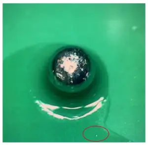
Based on the assessment in Table 2, the solder selected for the test meets Grade 1 standards; however, solder balls still form.
Therefore, it is inevitable that spatter from this solder during the soldering process will cause solder to adhere to non-soldered areas.
The test conditions did not specify key parameters such as heating rate, preheating, soak time, and reflow temperature. In actual production, operators strictly control these parameters, which significantly reduces the probability of solder bead spatter.
Moreover, industrial production rarely alters the solder system, so this factor does not serve as the primary cause of solder spatter.
From the perspective of the solder, it is possible to prevent solder splatter by modifying the film-forming agent in the flux—for example, using glyceryl stearate as the film-forming agent—so that the active substances form a uniform film on the printed circuit board after the solvent evaporates.
The mass fraction of the film-forming agent should be 1% to 2%.
Improvements
Based on the above analysis, solder moisture absorption is the primary cause of solder wetting during LTCC soldering.
Environmental temperature and humidity require strict monitoring during production, and operators must avoid exposing solder to air for extended periods after opening the can.
In general, production guidelines restrict the exposure time of printed circuit boards with applied solder to no more than 2 hours, while limiting solder paste exposure to no more than 4 hours.
Because solder must not adhere to bonding points on the LTCC surface, process control must strictly prevent spatter caused by moisture absorption during soldering, and operators must complete soldering immediately after paste application and component placement.
To address this issue, the production team changed the production mode for this product to single-piece flow and determined production parameters based on calculation results, including a production cycle of 127 s, a workshop temperature of 22.5–23.3 °C, and a relative humidity of 53.2%–54.7%.
After the production team continuously manufactured three batches of LTCC ceramic boards, they obtained the statistical results for solder contamination in non-soldering areas, as shown in Table 5.
| Batch | Inspected Points in Non-Soldered Area (pcs) | Solder-Adhered Points (pcs) | Solder Adhesion Rate (‰) |
|---|---|---|---|
| 1 | 5,250 | 7 | 1.33 |
| 2 | 6,600 | 9 | 1.36 |
| 3 | 5,050 | 6 | 1.19 |
Table 5. Statistical results of solder adhesion in non-soldering areas after improvement
As shown in Table 5, the proportion of unsoldered areas decreased significantly following the improvements, ideally dropping from 2.00‰ to 1.19‰.
These results indicate that optimizing production processes and strictly controlling temperature and humidity can effectively reduce solder moisture absorption and splatter, thereby significantly improving the assembly quality of surface-mount components on LTCC substrates.
These improvements not only enhance product reliability but also provide crucial process assurance for the application of LTCC technology in highly integrated, high-reliability electronic devices.
Conclusion
This paper presents an in-depth analysis and study of the issue of solder wetting on gold layers in non-soldering areas during the assembly of LTCC surface-mount components.
Experimental validation revealed that solder moisture absorption, inappropriate reflow profiles, and poor solder ball performance are the primary factors contributing to solder splatter.
In particular, the impact of solder moisture absorption is more pronounced in mixed-line production involving multiple product varieties and small batch sizes.
As the exposure time of the solder increases, the risk of moisture absorption rises, leading to a higher rate of solder wetting.
To address this issue, the paper proposes measures such as optimizing production processes, strictly controlling temperature and humidity, and improving the composition of flux and film-forming agents.
By implementing these improvements, the solder contamination rate in non-soldering areas decreased from 2.00‰ to 1.19‰–1.36‰, significantly enhancing the assembly quality of LTCC surface-mount components.
These research findings provide important technical optimization guidelines for the application of LTCC technology in highly integrated, high-reliability electronic devices.