PCB holes are a fundamental element in printed circuit board (PCB) design, playing a crucial role in enabling electrical connections, thermal management, and mechanical stability.
Understanding the different types of PCB holes and their specific functions is essential for designers and engineers who want to optimize PCB performance and reliability.
This article provides a detailed guide on the main types of PCB holes and their applications, helping readers deepen their knowledge of PCB manufacturing and design strategies.
Main Functions of Holes
1. Electrical Connection
Metallized Holes between copper layers could enable electrical connections. Depending on the type of holes, the processing method and function are different:
– Through Hole: Penetrates the entire PCB, used to connect the top and bottom layers of circuitry, and also for soldering through-hole components.
– Blind Via: In multilayer boards (4 layers and above), it connects from the outer layer (top and bottom layers) to the inner layers.
Primarily used for inner-layer signal transmission, it does not penetrate the entire PCB board and is widely used in high-density designs to improve space utilization within a limited area.
– Buried Via: Primarily used in multilayer boards (4 layers and above), it is entirely located between inner layers for signal transmission, improve wiring density and signal quality.
2. Thermal Dissipation
– Thermal vias: These metallized vias conduct heat from the bottom of components to other layers of the PCB or heatsinks, reducing localized heats and preventing thermal acceleration that might degrade performance during working, especially fully-loaded.
Widely applied for components in QFN/DFN packages, such as power management chips, RF modules, and MCUs.
3. Mechanical Mounting
– Component assembly and fixing holes: Used for soldering through-hole/DIP/THT components, such as electrolytic capacitors, connectors, relays, large inductors, transistors, and IGBT power transistors.
The hole diameter must match the component leads to ensure soldering reliability.
– Mounting holes: Typically located at the edge of the PCB, these are used to secure the board to the housing with screws, providing physical stability and grounding to reduce electromagnetic interference.
They are also used for mounting some auxiliary components, such as heatsink leads and IGBT power transistor leads.
Special Holes
» Slots

- Slots are typically manufactured by using methods such as mechanical drilling, mechanical shaping, and laser drilling/laser cutting.
- Elliptical Slot
- Square Slot


» Figure-8 Hole

- Equal-size Figure-8 Hole: The two circular holes forming the figure-8 hole which share the same diameter.
- Non-equal-size Figure-8 Hole: The two circular holes forming the figure-8 hole which have different diameters.
» Controlled-Depth Hole

- Controlled-depth holes are mechanically drilled, and are generally non-electroplated, lacking conductivity.
- Controlled-depth holes are commonly drilled from bottom side, hence the name “back drill.”
- Customers require different controlled depth based on their design and intendion. The common functions include heat dissipation and reducing interference.
- Considering the drill bit’s inertia during drilling, the thickness of the inner layer between the endpoint layer and the next layer in a controlled-depth hole is generally required to meet the tolerance requirements.
» Press-Fit Hole

- Press-Fit Hole: Mostly PTH holes, with strict diameter tolerances, typically +/-0.05mm.
- Press-fit technology: Also known as “fisheye terminal,” this technology is an alternative to soldering. It forms a connection by mating a flexible or rigid pin with a metallized hole on the PCB.
- Press-fit primarily achieves reliable electrical connections through a cold-connection, solderless method.
During the process, press the pins into the press-fit hole, the pin end undergoes elastic deformation and providing low contact resistance, then forge a highly reliable, tight connection.
» Countersink/Counterbore Hole


- Also known as stepped holes, funnel holes, or flared holes. Applied for screw mounting, typically where the top of the screw does not protrude excessively from the PCB surface.
- Function: Provides space below the PCB surface for the top of the screw, preventing the screw top from protruding.
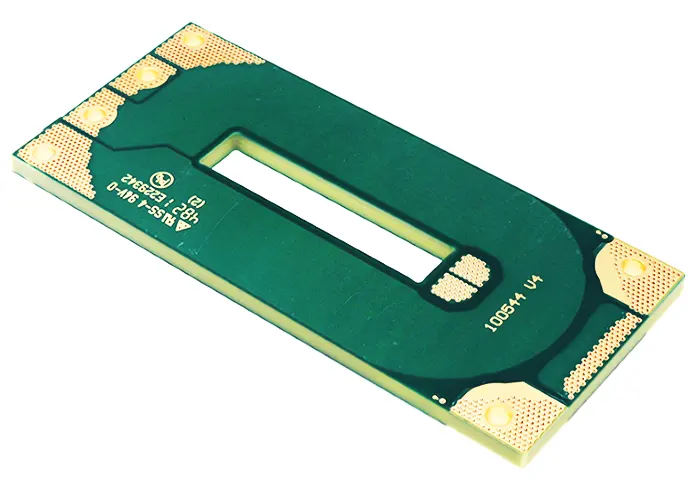
» Via-in-Pad


- A via, abbreviated as VIP or VOP, is a hole located under the pad.
- Vias are typically in diameter 0.5mm or less.
- After plating, vias are plugged with resin, and then a layer of copper is plated on top to cover them.
- Vias are hidden under the bottom of the pad and are primarily used for conductivity. (Figure 9)
- PCBs with VIP have relatively complex vias: The industry often uses the term “brush-after-brush,” meaning that after resin plugging, a brush smooths the resin surface of the VIP hole, followed by copper reduction.
After copper reduction, the resin in the VIP hole protrudes, so flating is required again to smooth the resin surface.
» PTH Half-Hole

- Modules widely use PTH half-holes for direct soldering onto the PCB, facilitating the application and integration of general-purpose modules.
- The difficulty in processing PTH half-holes is ensuring that the copper on another half of the hole does not peel off or lift while removing the other half.
» Satellite Holes


- A common positioning hole on PCBs, featuring a large central hole surrounded by 6 to 8 smaller holes.
- The large central hole is often an NPTH (NP-Through Hole).
» Extra-Large Hole

- Extra-large holes typically refer to drilled holes of 6 mm or larger, which CNC may form, especially when diameters exceed 6.5 mm.
» Stamp Hole

- Stamp holes are NPTH holes, commonly used in PCB panelization, as an alternative for V-cuts/V-groove, divide the individual boards conventiently.
- Advantages of stamp holes: could broke off the individuals manually without additional mechanical tools.
- Disadvantages of stamp-shaped holes: Uneven edges on the broken surface, prone to fiberglass residue, etc.
» Positioning Holes

- Usually NPTH holes.
- Function: To fix the PCB to the platform of SMT equipment.
- Location: Located on the processing edge of the PCB panel or on the PCB itself.
- Quantity: Usually 4.
The 11 types of holes above are common in PCB manufacturing and application.
Flexibly select the appropriate type based on the specific application scenario.
Shenzhen Benlida has been manufacturing PCB over 14 years.
With experience and investments, we have established an advanced production system. equipment, and professional engineers&technicians.
While committed to manufacturing PCB with excellent quality and service, we are also actively expanding and have built a strong supply chain for components.
If you need PCBs, components, or PCB assembly, please contact Benlida!
Conclusion
In summary, PCB holes are indispensable in modern PCB design and manufacturing.
From through holes and blind vias to specialized holes like press-fit or satellite holes, each type serves a specific purpose in improving connectivity, heat dissipation, and mechanical support.
By selecting the appropriate PCB holes for your project, you can ensure higher performance, reliability, and efficient use of board space.
Experienced manufacturers like Shenzhen Benlida leverage advanced production systems to deliver high-quality PCBs with the right hole configurations to meet diverse design requirements.